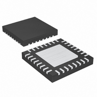
MAX3798ETJ+ Maxim Integrated Products, MAX3798ETJ+ Datasheet - Page 8

MAX3798ETJ+
Manufacturer Part Number
MAX3798ETJ+
Description
IC LIMITING AMP/VCSEL DVR 32TQFN
Manufacturer
Maxim Integrated Products
Datasheet
1.MAX3798ETJ.pdf
(35 pages)
Specifications of MAX3798ETJ+
Amplifier Type
Limiting
Number Of Circuits
1
Output Type
Differential
Current - Supply
97mA
Voltage - Supply, Single/dual (±)
2.85 V ~ 3.63 V
Operating Temperature
-40°C ~ 85°C
Mounting Type
Surface Mount
Package / Case
32-TQFN Exposed Pad
Operating Temperature Range
+ 85 C
Mounting Style
SMD/SMT
Lead Free Status / RoHS Status
Lead free / RoHS Compliant
Current - Output / Channel
-
-3db Bandwidth
-
Slew Rate
-
Gain Bandwidth Product
-
Current - Input Bias
-
Voltage - Input Offset
-
Lead Free Status / Rohs Status
Details
1.0625Gbps to 10.32Gbps, Integrated, Low-
Power SFP+ Limiting Amplifier and VCSEL Driver
Figure 1. Test Circuit for VCSEL Driver Characterization
Note 5: Receiver deterministic jitter is measured with a repeating 2
Note 6: Measured with a k28.5 pattern from 1.0625Gbps to 8.5Gbps. Measured with 2
Note 7: Measurement includes an input AC-coupling capacitor of 100nF and C
Note 8: Gain stability is defined as [(I_measured) - (I_reference)]/(I_reference) over the listed current range, temperature, and V
Note 9: Transmitter deterministic jitter is measured with a repeating 2
Note 10: Gain stability is defined as [(I_measured) - (I_reference)]/(I_reference) over the listed current range, temperature, and V
8
_______________________________________________________________________________________
8.5Gbps, a repeating K28.5 pattern [00111110101100000101] is used. Deterministic jitter is defined as the arithmetic sum
of pulse-width distortion (PWD) and pattern-dependent jitter (PDJ).
between two amplitudes: Signal_ON and Signal_OFF.
1) Receiver operates at sensitivity level plus 1dB power penalty.
2) Receiver operates at overload.
max_deassert_level and the min_assert_level are measured for one LOS_THRESHOLD setting.
from +2.95V to +3.63V. Reference current measured at V
10.32Gbps. For 1.0625Gbps to 8.5Gbps, a repeating K28.5 pattern [00111110101100000101] is used. Deterministic jitter is
defined as the arithmetic sum of PWD and PDJ.
from +2.85V to +3.63V. Reference current measured at V
a) Signal_OFF = 0
b) Signal_ON = (+1dB) + 10log(max_deassert_level)
Signal_OFF = 0
Signal_ON = 1.2V
Signal_ON = (+8dB) + 10log(min_assert_level)
Signal_OFF = 0
V
CC
OSCILLOSCOPE
CONTROLLER
0.1μF
50Ω
50Ω
P-P
1μH
V
CONTROLLER
50Ω
50Ω
CCR
1000pF
4.7kΩ
V
0.1μF
V
CCR
0.1μF
0.1μF
CCD
V
V
V
1000pF
CCR
CCT
CCD
V
LOS
MSEL
ROUT+
ROUT-
DISABLE
V
CCR
CCD
CONTROLLER
1nF
MAX3798
CC
CC
0.1μF
0.1μF
31
= +3.2V, T
= +3.3V, T
7
- 1 PRBS equivalent pattern at 10.32Gbps. For 1.0625Gbps to
- 1 PRBS, 72 0s, 2
0.1μF
0.1μF
CAZ
V
A
A
CCT
= +25°C.
= +25°C.
1kΩ
TOUT+
FAULT
TOUT-
400Ω
BMAX
V
BIAS
V
V
of 100nF. The signal at the input is switched
CCT
EER
EET
31
- 1 PRBS at 10.32Gbps.
7
0.1μF
0.1μF
V
CCT
- 1 PRBS, and 72 1s pattern at
CONTROLLER
1000pF
400Ω
V
CCT
50Ω
50Ω
4.7kΩ
OSCILLOSCOPE
50Ω
50Ω
CC
CC


