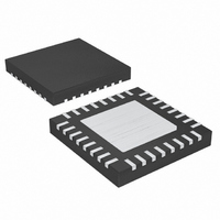
MAX3798ETJ+ Maxim Integrated Products, MAX3798ETJ+ Datasheet - Page 28

MAX3798ETJ+
Manufacturer Part Number
MAX3798ETJ+
Description
IC LIMITING AMP/VCSEL DVR 32TQFN
Manufacturer
Maxim Integrated Products
Datasheet
1.MAX3798ETJ.pdf
(35 pages)
Specifications of MAX3798ETJ+
Amplifier Type
Limiting
Number Of Circuits
1
Output Type
Differential
Current - Supply
97mA
Voltage - Supply, Single/dual (±)
2.85 V ~ 3.63 V
Operating Temperature
-40°C ~ 85°C
Mounting Type
Surface Mount
Package / Case
32-TQFN Exposed Pad
Operating Temperature Range
+ 85 C
Mounting Style
SMD/SMT
Lead Free Status / RoHS Status
Lead free / RoHS Compliant
Current - Output / Channel
-
-3db Bandwidth
-
Slew Rate
-
Gain Bandwidth Product
-
Current - Input Bias
-
Voltage - Input Offset
-
Lead Free Status / Rohs Status
Details
1.0625Gbps to 10.32Gbps, Integrated, Low-
Power SFP+ Limiting Amplifier and VCSEL Driver
impromptu deemphasis adjustment, it is recommended
that the DE_INC (MODINC[5]) bit is used. Use of this bit
increments or decrements the deemphasis code setting
by 1 LSB based on the sign of increment in the
MODINC[4:0] and, hence, the SET_IMOD[8:0] setting.
This helps maintain the BER while having the flexibility to
improve signal quality by adjusting deemphasis while
the transmit operation continues. This feature enables
glitchless deemphasis adjustment while maintaining
excellent BER performance.
The eye crossing at the Tx output can be adjusted
using the SET_PWCTRL register. Table 6 shows these
settings.
The sign of the number specifies the direction of pulse-
width distortion. The code of 1111 corresponds to a
balanced state for differential output. The pulse-width
distortion is bidirectional around the balanced state
(see the Typical Operating Characteristics section).
Table 6. Eye-Crossing Settings for
SET_PWCTRL
Amplitude of the CML output stage is controlled by an
8-bit DAC register (SET_CML). The differential output
amplitude range is from 40mV
4.6mV
tial load).
For AC-coupling, the coupling capacitors C
C
28
Output Voltage R
SET_PWCTRL[3:0]
OUT
______________________________________________________________________________________
P-P
should be selected to minimize the receiver’s
1000
1001
1010
1011
1100
1101
1110
1111
resolution (assuming an ideal 100Ω differen-
Programming CML Output Settings
Programming Pulse-Width Control
Select the Coupling Capacitor
OUT
PWD
(mV
-7
-6
-5
-4
-3
-2
-1
0
P-P
SET_PWCTRL[3:0]
) = 40 + 4.55 (SET_CML)
P-P
up to 1200mV
0111
0110
0101
0100
0011
0010
0001
0000
P-P
IN
PWD
8
7
6
5
4
3
2
1
and
with
deterministic jitter. Jitter is decreased as the input low-
frequency cutoff (f
The recommended C
MAX3798.
The capacitor between CAZ1 and CAZ2 determines the
time constant of the signal path DC-offset cancellation
loop. To maintain stability, it is important to keep at
least a one-decade separation between f
low-frequency cutoff (f
set cancellation circuit. A 1nF capacitor between CAZ1
and CAZ2 is recommended for the MAX3798.
To minimize inductance, keep the connections between
the MAX3798 output pins and laser diode as close as
possible. Optimize the laser diode performance by
placing a bypass capacitor as close as possible to the
laser anode. Use good high-frequency layout tech-
niques and multiple-layer boards with uninterrupted
ground planes to minimize EMI and crosstalk.
The exposed pad on the 32-pin TQFN provides a very
low-thermal resistance path for heat removal from the IC.
The pad is also electrical ground on the MAX3798 and
must be soldered to the circuit board ground for proper
thermal and electrical performance. Refer to Application
Note 862: HFAN-08.1: Thermal Considerations of QFN
and Other Exposed-Paddle Packages for additional
information.
Using the MAX3798 laser driver alone does not ensure
that a transmitter design is compliant with IEC 825. The
entire transmitter circuit and component selections
must be considered. Each user must determine the
level of fault tolerance required by the application, rec-
ognizing that Maxim products are neither designed nor
authorized for use as components in systems intended
for surgical implant into the body, for applications
intended to support or sustain life, or for any other
application in which the failure of a Maxim product
could create a situation where personal injury or death
could occur.
Select the Offset-Correction Capacitor
Applications Information
f
IN
IN
) is decreased.
= 1/[2π(50)(C
OC
Laser Safety and IEC 825
IN
) associated with the DC-off-
and C
Layout Considerations
Exposed-Pad Package
OUT
IN
)]
is 0.1μF for the
IN
and the


