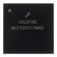
MCF5282CVM80 Freescale Semiconductor, MCF5282CVM80 Datasheet - Page 50

MCF5282CVM80
Manufacturer Part Number
MCF5282CVM80
Description
IC MPU 512K 80MHZ 256-MAPBGA
Manufacturer
Freescale Semiconductor
Series
MCF528xr
Datasheet
1.MCF5216CVM66J.pdf
(766 pages)
Specifications of MCF5282CVM80
Core Processor
Coldfire V2
Core Size
32-Bit
Speed
80MHz
Connectivity
CAN, EBI/EMI, Ethernet, I²C, SPI, UART/USART
Peripherals
DMA, LVD, POR, PWM, WDT
Number Of I /o
150
Program Memory Size
512KB (512K x 8)
Program Memory Type
FLASH
Ram Size
64K x 8
Voltage - Supply (vcc/vdd)
2.7 V ~ 3.6 V
Data Converters
A/D 8x10b
Oscillator Type
External
Operating Temperature
-40°C ~ 85°C
Package / Case
256-MAPBGA
Controller Family/series
ColdFire
Ram Memory Size
64KB
Embedded Interface Type
CAN, I2C, SPI, UART
No. Of Pwm Channels
8
Digital Ic Case Style
MAPBGA
Rohs Compliant
Yes
Lead Free Status / RoHS Status
Lead free / RoHS Compliant
Eeprom Size
-
Available stocks
Company
Part Number
Manufacturer
Quantity
Price
Company:
Part Number:
MCF5282CVM80
Manufacturer:
FREESCALE
Quantity:
1 831
Company:
Part Number:
MCF5282CVM80
Manufacturer:
Freescale Semiconductor
Quantity:
10 000
Company:
Part Number:
MCF5282CVM80J
Manufacturer:
Freescale Semiconductor
Quantity:
10 000
- Current page: 50 of 766
- Download datasheet (9Mb)
ColdFire Core
2.2.1
D0–D7 data registers are for bit (1-bit), byte (8-bit), word (16-bit) and longword (32-bit) operations; they
can also be used as index registers.
2.2.2
These registers can be used as software stack pointers, index registers, or base address registers. They can
also be used for word and longword operations.
2-4
1
The values listed in this column represent the Rc field used when accessing the core registers via the BDM port. For more
information see
0x004–5
0x80F
0x80E
0xC04
0xC05
BDM
0x002
0x800
0x801
(D0, D1)
(D2-D7)
Reset
Reset
BDM: Load: 0x080 + n; n = 0-7 (Dn)
1
W
R
Data Registers (D0–D7)
Address Registers (A0–A6)
Store: 0x180 + n; n = 0-7 (Dn)
31 30 29 28 27 26 25 24 23 22 21 20 19 18 17 16 15 14 13 12 11 10 9
– – – – – – – – – – – – – – – – – – – – – – – – – – – – – – – –
Registers D0 and D1 contain hardware configuration details after reset. See
Section 2.3.4.15, “Reset Exception”
Chapter 30, “Debug
Program Counter (PC)
Cache Control Register (CACR)
Access Control Register 0–1 (ACR0–1)
User/Supervisor A7 Stack Pointer
(OTHER_A7)
Vector Base Register (VBR)
Status Register (SR)
Flash Base Address Register
(FLASHBAR)
RAM Base Address Register (RAMBAR)
Table 2-1. ColdFire Core Programming Model (continued)
MCF5282 and MCF5216 ColdFire Microcontroller User’s Manual, Rev. 3
Register
Support”.
Figure 2-2. Data Registers (D0–D7)
Supervisor Access Only Registers
See
Section 2.3.4.15, “Reset Exception”
NOTE
for more details.
Width
(bits)
32
32
32
32
32
16
32
32
Data
Access
R/W
R/W
R/W
R/W
R/W
R/W
R/W
R/W
0x0000_0004
0x0000_0000
0x0000_0000
0x0000_0000
0x0000_0000
Reset Value
See Section
See Section
Contents of
Contents of
location
location
0x27--
8
7
Access: User read/write
Written with
6
MOVEC
Freescale Semiconductor
Yes
Yes
Yes
Yes
Yes
No
No
No
5
BDM read/write
4
3
Section/Page
2
2.2.10/2-8
2.2.10/2-8
2.2.5/2-7
2.2.6/2-7
2.2.7/2-7
2.2.3/2-5
2.2.8/2-7
2.2.9/2-8
1
0
Related parts for MCF5282CVM80
Image
Part Number
Description
Manufacturer
Datasheet
Request
R
Part Number:
Description:
Mcf5282 And Mcf5216 Coldfire Microcontroller User�s Manual
Manufacturer:
Freescale Semiconductor, Inc
Datasheet:
Part Number:
Description:
Manufacturer:
Freescale Semiconductor, Inc
Datasheet:
Part Number:
Description:
Manufacturer:
Freescale Semiconductor, Inc
Datasheet:
Part Number:
Description:
Manufacturer:
Freescale Semiconductor, Inc
Datasheet:
Part Number:
Description:
Manufacturer:
Freescale Semiconductor, Inc
Datasheet:
Part Number:
Description:
Manufacturer:
Freescale Semiconductor, Inc
Datasheet:
Part Number:
Description:
Manufacturer:
Freescale Semiconductor, Inc
Datasheet:
Part Number:
Description:
Manufacturer:
Freescale Semiconductor, Inc
Datasheet:
Part Number:
Description:
Manufacturer:
Freescale Semiconductor, Inc
Datasheet:
Part Number:
Description:
Manufacturer:
Freescale Semiconductor, Inc
Datasheet:
Part Number:
Description:
Manufacturer:
Freescale Semiconductor, Inc
Datasheet:
Part Number:
Description:
Manufacturer:
Freescale Semiconductor, Inc
Datasheet:
Part Number:
Description:
Manufacturer:
Freescale Semiconductor, Inc
Datasheet:
Part Number:
Description:
Manufacturer:
Freescale Semiconductor, Inc
Datasheet:
Part Number:
Description:
Manufacturer:
Freescale Semiconductor, Inc
Datasheet:


