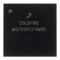
MCF5282CVM80 Freescale Semiconductor, MCF5282CVM80 Datasheet - Page 741

MCF5282CVM80
Manufacturer Part Number
MCF5282CVM80
Description
IC MPU 512K 80MHZ 256-MAPBGA
Manufacturer
Freescale Semiconductor
Series
MCF528xr
Datasheet
1.MCF5216CVM66J.pdf
(766 pages)
Specifications of MCF5282CVM80
Core Processor
Coldfire V2
Core Size
32-Bit
Speed
80MHz
Connectivity
CAN, EBI/EMI, Ethernet, I²C, SPI, UART/USART
Peripherals
DMA, LVD, POR, PWM, WDT
Number Of I /o
150
Program Memory Size
512KB (512K x 8)
Program Memory Type
FLASH
Ram Size
64K x 8
Voltage - Supply (vcc/vdd)
2.7 V ~ 3.6 V
Data Converters
A/D 8x10b
Oscillator Type
External
Operating Temperature
-40°C ~ 85°C
Package / Case
256-MAPBGA
Controller Family/series
ColdFire
Ram Memory Size
64KB
Embedded Interface Type
CAN, I2C, SPI, UART
No. Of Pwm Channels
8
Digital Ic Case Style
MAPBGA
Rohs Compliant
Yes
Lead Free Status / RoHS Status
Lead free / RoHS Compliant
Eeprom Size
-
Available stocks
Company
Part Number
Manufacturer
Quantity
Price
Company:
Part Number:
MCF5282CVM80
Manufacturer:
FREESCALE
Quantity:
1 831
Company:
Part Number:
MCF5282CVM80
Manufacturer:
Freescale Semiconductor
Quantity:
10 000
Company:
Part Number:
MCF5282CVM80J
Manufacturer:
Freescale Semiconductor
Quantity:
10 000
- Current page: 741 of 766
- Download datasheet (9Mb)
B.3
Freescale Semiconductor
Table 33-27 on page
Table 33-27 on page
Table 33-27 on page
Table 33-27 on page
Table 33-27 on page
Table 33-27 on page
Table 33-27 on page
Table 33-28 on page
Table 33-28 on page
Throughout Manual Added MCF5281 device to manual. The MCF5281 implements half the Flash of the MCF5282.
Table A-3 on page
Table 6-12/6-16
Table 6-13/6-20
Figure 6-2/6-4
Table 2-2/2-7
Table 5-1/5-2
Table 5-1/5-3
33.13/33-21
Location
Location
1.1/1-1
33-25
33-25
33-25
33-25
33-25
33-25
33-25
33-27
33-27
A-3
Changes Between Rev. 1 and Rev. 2
Added timing diagrams and tables to
Changed the max value in spec 1 to “1/4.”
Changed the min value in spec 2 to “4.”
Changed the min value in spec 3 to “25.”
Changed the min value in spec 6 to “25.”
Changed the max value in spec 7 to “30.”
Changed the max value in spec 8 to “30.”
Changed the max value in spec 11 to “25.”
Changed the min value in spec D1 to “5.”
Changed the min value in spec D2 to “2.”
Changed offset for the copy of RAMBAR to “0x008.”
Replaced Figure 6-2, “CFM 512K Array Memory Map” and renamed it “CFM Array Memory Map”
Changed the description of real time debug support. It has only one user-visible hardware breakpoint
register.
Change the I field description to read: “Interrupt level mask. Defines the current interrupt level. Interrupt
requests are inhibited for all priority levels less than or equal to the current level, except the edge-sensitive
level 7 request, which cannot be masked.”
Replaced the description of PRI1 and PRI2.
Added note to the SPV bit description, “The BDE bit in the second RAMBAR register must also be set to
allow dual port access to the SRAM. For more information, see Section 8.4.2, ‘Memory Base Address
Register (RAMBAR).’”
Change value for page erase verify command to 0x06.
Change value for page erase verify command to 0x06.
MCF5282 and MCF5216 ColdFire Microcontroller User’s Manual, Rev. 3
Table B-2. Rev. 0.1 to Rev. 1 Changes (continued)
Table B-3. Rev. 1 to Rev. 2 Changes
Section 33.13, “Fast Ethernet AC Timing
Description
Description
Specifications.”
Revision History
B-5
Related parts for MCF5282CVM80
Image
Part Number
Description
Manufacturer
Datasheet
Request
R
Part Number:
Description:
Mcf5282 And Mcf5216 Coldfire Microcontroller User�s Manual
Manufacturer:
Freescale Semiconductor, Inc
Datasheet:
Part Number:
Description:
Manufacturer:
Freescale Semiconductor, Inc
Datasheet:
Part Number:
Description:
Manufacturer:
Freescale Semiconductor, Inc
Datasheet:
Part Number:
Description:
Manufacturer:
Freescale Semiconductor, Inc
Datasheet:
Part Number:
Description:
Manufacturer:
Freescale Semiconductor, Inc
Datasheet:
Part Number:
Description:
Manufacturer:
Freescale Semiconductor, Inc
Datasheet:
Part Number:
Description:
Manufacturer:
Freescale Semiconductor, Inc
Datasheet:
Part Number:
Description:
Manufacturer:
Freescale Semiconductor, Inc
Datasheet:
Part Number:
Description:
Manufacturer:
Freescale Semiconductor, Inc
Datasheet:
Part Number:
Description:
Manufacturer:
Freescale Semiconductor, Inc
Datasheet:
Part Number:
Description:
Manufacturer:
Freescale Semiconductor, Inc
Datasheet:
Part Number:
Description:
Manufacturer:
Freescale Semiconductor, Inc
Datasheet:
Part Number:
Description:
Manufacturer:
Freescale Semiconductor, Inc
Datasheet:
Part Number:
Description:
Manufacturer:
Freescale Semiconductor, Inc
Datasheet:
Part Number:
Description:
Manufacturer:
Freescale Semiconductor, Inc
Datasheet:


