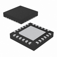
ATA5773-PXQW Atmel, ATA5773-PXQW Datasheet - Page 60

ATA5773-PXQW
Manufacturer Part Number
ATA5773-PXQW
Description
XMITTR UHF ASK/FSK 310MHZ 24VQFN
Manufacturer
Atmel
Datasheet
1.ATA5773-DK1.pdf
(219 pages)
Specifications of ATA5773-PXQW
Frequency
310MHz ~ 350MHz
Modulation Or Protocol
UHF
Power - Output
8dBm
Voltage - Supply
2 V ~ 4 V
Current - Transmitting
9.8mA
Data Interface
PCB, Surface Mount
Memory Size
4kB Flash, 256B EEPROM, 256B SRAM
Antenna Connector
PCB, Surface Mount
Operating Temperature
-40°C ~ 85°C
Package / Case
24-VQFN Exposed Pad, 24-HVQFN, 24-SQFN, 24-DHVQFN
Processor Series
ATA5x
Core
AVR8
Data Bus Width
8 bit
Program Memory Type
Flash
Program Memory Size
4 KB
Data Ram Size
256 B
Interface Type
SPI, USI
Maximum Clock Frequency
4 MHz
Number Of Programmable I/os
12
Number Of Timers
2
Maximum Operating Temperature
+ 85 C
Mounting Style
SMD/SMT
Minimum Operating Temperature
- 40 C
On-chip Adc
10 bit, 12 Channel
Lead Free Status / RoHS Status
Lead free / RoHS Compliant
Applications
-
Sensitivity
-
Data Rate - Maximum
-
Current - Receiving
-
Lead Free Status / Rohs Status
Details
Available stocks
Company
Part Number
Manufacturer
Quantity
Price
Company:
Part Number:
ATA5773-PXQW
Manufacturer:
ATMEL
Quantity:
3 500
Part Number:
ATA5773-PXQW
Manufacturer:
ATMEL/爱特梅尔
Quantity:
20 000
- Current page: 60 of 219
- Download datasheet (4Mb)
4.13.2.5
4.14
4.14.1
60
I/O Ports
Atmel ATA5771/73/74
Overview
PCMSK0 – Pin Change Mask Register 0
• Bits 7..0 – PCINT7..0: Pin Change Enable Mask 7..0
Each PCINT7..0 bit selects whether pin change interrupt is enabled on the corresponding I/O
pin. If PCINT7..0 is set and the PCIE0 bit in GIMSK is set, pin change interrupt is enabled on
the corresponding I/O pin. If PCINT7..0 is cleared, pin change interrupt on the corresponding
I/O pin is disabled.
All AVR
ports. This means that the direction of one port pin can be changed without unintentionally
changing the direction of any other pin with the SBI and CBI instructions. The same applies
when changing drive value (if configured as output) or enabling/disabling of pull-up resistors (if
configured as input). Each output buffer has symmetrical drive characteristics with both high
sink and source capability. The pin driver is strong enough to drive LED displays directly. All
port pins have individually selectable pull-up resistors with a supply-voltage invariant resis-
tance. All I/O pins have protection diodes to both V
See
Figure 4-21. I/O Pin Equivalent Schematic
All registers and bit references in this section are written in general form. A lower case “x” rep-
resents the numbering letter for the port, and a lower case “n” represents the bit number.
However, when using the register or bit defines in a program, the precise form must be used.
For example, PORTB3 for bit no. 3 in Port B, here documented generally as PORTxn. The
physical I/O Registers and bit locations are listed in
Bit
0x12 (0x32)
Read/Write
Initial Value
Section 8. “Electrical Characteristics” on page 186
®
ports have true Read-Modify-Write functionality when used as general digital I/O
Pxn
PCINT7
R/W
7
0
PCINT6
R/W
6
0
PCINT5
C
R/W
5
0
pin
PCINT4
R/W
4
0
PCINT3
CC
R/W
Table
3
0
and Ground as indicated in
for a complete list of parameters.
"General Digital I/O" for
4-29.
PCINT2
R/W
2
0
See Figure
R
Details
pu
PCINT1
R/W
1
0
Logic
PCINT0
R/W
0
0
9137E–RKE–12/10
Figure
PCMSK0
4-21.
Related parts for ATA5773-PXQW
Image
Part Number
Description
Manufacturer
Datasheet
Request
R

Part Number:
Description:
BOARD XMITTER FOR ATA5773 315MHZ
Manufacturer:
Atmel
Datasheet:

Part Number:
Description:
Microcontroller With Uhf Ask/fsk Transmitter
Manufacturer:
ATMEL Corporation
Datasheet:

Part Number:
Description:
DEV KIT FOR AVR/AVR32
Manufacturer:
Atmel
Datasheet:

Part Number:
Description:
INTERVAL AND WIPE/WASH WIPER CONTROL IC WITH DELAY
Manufacturer:
ATMEL Corporation
Datasheet:

Part Number:
Description:
Low-Voltage Voice-Switched IC for Hands-Free Operation
Manufacturer:
ATMEL Corporation
Datasheet:

Part Number:
Description:
MONOLITHIC INTEGRATED FEATUREPHONE CIRCUIT
Manufacturer:
ATMEL Corporation
Datasheet:

Part Number:
Description:
AM-FM Receiver IC U4255BM-M
Manufacturer:
ATMEL Corporation
Datasheet:

Part Number:
Description:
Monolithic Integrated Feature Phone Circuit
Manufacturer:
ATMEL Corporation
Datasheet:

Part Number:
Description:
Multistandard Video-IF and Quasi Parallel Sound Processing
Manufacturer:
ATMEL Corporation
Datasheet:

Part Number:
Description:
High-performance EE PLD
Manufacturer:
ATMEL Corporation
Datasheet:

Part Number:
Description:
8-bit Flash Microcontroller
Manufacturer:
ATMEL Corporation
Datasheet:

Part Number:
Description:
2-Wire Serial EEPROM
Manufacturer:
ATMEL Corporation
Datasheet:


