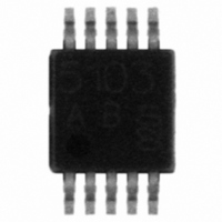
TDA5150 Infineon Technologies, TDA5150 Datasheet - Page 60

TDA5150
Manufacturer Part Number
TDA5150
Description
IC TX MULTI-CH/BAND 10-TSSOP
Manufacturer
Infineon Technologies
Type
Multiband Transmitterr
Datasheet
1.TDA5150.pdf
(106 pages)
Specifications of TDA5150
Package / Case
10-TSSOP
Frequency
300MHz ~ 320MHz, 425MHz ~ 450MHz, 863MHz ~ 928MHz
Applications
RKE, Security Systems
Modulation Or Protocol
ASK, FSK, GFSK
Data Rate - Maximum
50 kbps
Power - Output
10dBm
Current - Transmitting
16mA
Data Interface
PCB, Surface Mount
Antenna Connector
PCB, Surface Mount
Voltage - Supply
1.9 V ~ 3.6 V
Operating Temperature
-40°C ~ 85°C
Maximum Operating Temperature
+ 85 C
Mounting Style
SMD/SMT
Supply Current
16 mA
Supply Voltage (max)
3.6 V
Supply Voltage (min)
1.9 V
Lead Free Status / RoHS Status
Lead free / RoHS Compliant
Features
-
Memory Size
-
Lead Free Status / RoHS Status
Lead free / RoHS Compliant, Lead free / RoHS Compliant
Other names
SP000300415
TDA5150
TDA5150INTR
TDA5150
TDA5150INTR
Available stocks
Company
Part Number
Manufacturer
Quantity
Price
•
•
•
– Modulation type (ASK or FSK) is controlled by bit-field ASKFSK1:2
– RF-PA block activation, controlled by bit-fields PA_PS1
– RF-PA output power selection, controlled by the bit-fields POUT1
– If D=0, following fields are selected: [ASKFSK1, together with PA_PS1 and POUT1].
•
After the transmit command have been sent, the SCLK line has to stay low for at least
100 µs (i.e settling time of the PLL). A rising edge of the SCLK line after this brake
activates the PA and starts the transmission. The digital data is input into the transmitter
via the SDIO line and transposed into modulated RF signal, without regard on the state
of SCLK line (which could be Low or High).
To keep crosstalk between SCLK and SDIO at minimum level, it is recommended to
keep SCLK at a steady level, instead of toggling it (usually by the uC).
Data Sheet
SFR Transmitter Configuration Register 1 (0x05). The modulation type selection is
done individually for each of the two transmission settings (steered by bit D=0 or D=1),
with choice between ASK and FSK modulation. The settings are not coupled, i.e one
could be set for ASK modulation and the other for FSK for example. Further, if FSK is
chosen as modulation type, enabling of Gaussian filtering is another option - but not
mandatory. See also
and Data
PA_PS2
two transmission settings
respectively POUT2
(0x1B)
If D=1, following fields are selected: [ASKFSK2, together with PA_PS2 and POUT2].
B: If 0, the PA is switched off by the falling edge of the EN line. If 1, the SDIO line is
latched with the falling edge of EN, the PA stays active, continuing to transmit
according to the latched SDIO state. After a time-out duration of 65536 / f
for a 13 MHz reference clock), both the PA and PLL are switched off if no other SPI
command starts a new transmission. This feature helps to keep the transmitter
sending, despite the fact that the EN line is pulled to Low state, normally a stop
condition for Transmitter. Pulling the EN line to (Low) in between SPI command
blocks is required by SPI protocol, if commands are not sent in burst mode.
C: If C=0, the Encoder is not used. If C=1, the Encoder is used as configured in the
Transmitter Configuration Register 1, bits ENCMODE (0x05.2:0).
D: Switch between two subsets of transmission parameters, referenced as
PowerLevel/Modulation Setting n. Each subset contains 3 bit-fields for control of:
– modulation type (ASK or FSK)
– RF-PA block activation (3 blocks are available, may be switched ON/OFF individually)
– RF-PA output power
E, F RF Frequency selection as configured in PLL MM Integer Value registers
A/B/C/D
A/B/C/D
for the two transmission settings
(0x1A.7:5)
(0x0A:0x0C/0x0E:0x10/0x12:0x14/0x16:0x18.
Encoding.
(0x09/0x0D/0x11/0x15)
of the SFR Output Power Configuration Register 0,
(0x1B.7:4)
Chapter 2.4.4.2 SFRs related to Transmitter Configuration
of the SFR Output Power Configuration Register 1,
and the PLL Fractional Division Ratio registers
60
TDA 5150 Functional Description
(0x1A.4:2)
(0x05.6:5)
V 1.0, July 2009
(0x1A)
respectively
TDA 5150
(0x1B.3:0)
sys
(~5 ms
for the
of the


