FDME1024NZT Fairchild Semiconductor, FDME1024NZT Datasheet

MOSFET N-CH 20V 3.8A 6-MICROFET

FDME1024NZT

Manufacturer Part Number
FDME1024NZT
Description
MOSFET N-CH 20V 3.8A 6-MICROFET
Manufacturer
Fairchild Semiconductor
Series
PowerTrench®r
Datasheet

Specifications of FDME1024NZT

Fet Type
2 N-Channel (Dual)
Fet Feature
Logic Level Gate
Rds On (max) @ Id, Vgs
66 mOhm @ 3.4A, 4.5V
Drain To Source Voltage (vdss)
20V
Current - Continuous Drain (id) @ 25° C
3.8A
Vgs(th) (max) @ Id
1V @ 250µA
Gate Charge (qg) @ Vgs
4.2nC @ 4.5V
Input Capacitance (ciss) @ Vds
300pF @ 10V
Power - Max
600mW
Mounting Type
Surface Mount
Package / Case
6-MLP, 6-MicroFET™
Configuration
Single
Transistor Polarity
N-Channel
Resistance Drain-source Rds (on)
55 mOhms
Drain-source Breakdown Voltage
20 V
Continuous Drain Current
3.4 A
Power Dissipation
1.3 W
Maximum Operating Temperature
+ 150 C
Forward Transconductance Gfs (max / Min)
9 S
Gate Charge Qg
3 nC
Minimum Operating Temperature
- 55 C
Mounting Style
SMD/SMT
Lead Free Status / RoHS Status
Lead free / RoHS Compliant

Available stocks

Company
Part Number
Manufacturer
Quantity
Price
Part Number:
FDME1024NZT
0
©2010 Fairchild Semiconductor Corporation
FDME1024NZT Rev.C1
FDME1024NZT
Dual N-Channel PowerTrench
20 V, 3.8 A, 66 mΩ
Features
MOSFET Maximum Ratings
Thermal Characteristics
Package Marking and Ordering Information
V
V
I
P
T
R
R
Pin 1
D
DS
GS
D
J
θJA
θJA
Max r
Max r
Max r
Max r
Low profile:
MicroFET 1.6x1.6 Thin
Free from halogenated compounds and antimony oxides
HBM ESD protection level > 1600 V (Note 3)
RoHS Compliant
, T
Symbol
Device Marking
STG
DS(on)
DS(on)
DS(on)
DS(on)
S1
4T
G1
= 66 mΩ at V
= 86 mΩ at V
= 113 mΩ at V
= 160 mΩ at V
BOTTOM
Drain to Source Voltage
Gate to Source Voltage
Drain Current -Continuous
Power Dissipation for Single Operation
Operating and Storage Junction Temperature Range
Thermal Resistance, Junction to Ambient (Single Operation)
0.55 mm maximum in the new package
D2
D1
GS
GS
D2
GS
GS
FDME1024NZT
= 4.5 V, I
= 2.5 V, I
MicroFET 1.6x1.6 Thin
D1
= 1.8 V, I
= 1.5 V, I
-Pulsed
Device
G2
D
D
D
D
S2
= 3.4 A
= 2.9 A
= 2.5 A
= 2.1 A
T
A
= 25 °C unless otherwise noted
MicroFET 1.6x1.6 Thin
Parameter
®
Package
MOSFET
T
T
T
A
A
A
= 25 °C
= 25 °C
= 25 °C
TOP
1
General Description
This device is designed specifically as a single package solution
for dual switching requirement in cellular handset and other
ultra-portable
N-Channel MOSFETs with low on-state resistance for minimum
conduction losses.
The MicroFET 1.6x1.6 Thin package offers exceptional thermal
performance for it's physical size and is well suited to switching
and linear mode applications.
Applications
Baseband Switch
Load Switch
Reel Size
7 ’’
applications.
(Note 1a)
(Note 1a)
(Note 1b)
(Note 1a)
(Note 1b)
Tape Width
It
8 mm
features
-55 to +150
Ratings
195
3.8
1.4
0.6
90
20
±8
6
two
www.fairchildsemi.com
July 2010
5000 units
Quantity
independent
Units
°C/W
°C
W
V
V
A

Related parts for FDME1024NZT

FDME1024NZT Summary of contents

Page 1

... Thermal Resistance, Junction to Ambient (Single Operation) θJA Package Marking and Ordering Information Device Marking Device 4T FDME1024NZT ©2010 Fairchild Semiconductor Corporation FDME1024NZT Rev.C1 ® MOSFET General Description = 3.4 A This device is designed specifically as a single package solution D for dual switching requirement in cellular handset and other = 2 ...

Page 2

... Pulse Test: Pulse Width < 300 μs, Duty cycle < 2.0%. 3. The diode connected between the gate and source serves only as protection ESD. No gate overvoltage rating is implied. FDME1024NZT Rev. °C unless otherwise noted J Test Conditions = 250 μ ...

Page 3

... Junction Temperature 6 μ PULSE DURATION = 80 s DUTY CYCLE = 0.5% MAX 150 0.0 0.5 1 GATE TO SOURCE VOLTAGE (V) GS Figure 5. Transfer Characteristics FDME1024NZT Rev. °C unless otherwise noted J 3 2.5 V 2.5 = 1.8 V 2.0 = 1.5 V 1.5 μ s 1.0 0.5 1.0 1.5 300 250 200 ...

Page 4

... LIMITED BY r DS(on) 0.1 SINGLE PULSE T = MAX RATED 195 C/W θ 0.01 0 DRAIN to SOURCE VOLTAGE (V) DS Figure 9. Forward Bias Safe Operating Area 100 Figure 11. Single Pulse Maximum Power Dissipation FDME1024NZT Rev. °C unless otherwise noted J 500 = 8 V 100 μ 100 100 ...

Page 5

... Typical Characteristics 2 DUTY CYCLE-DESCENDING ORDER 0.5 0.2 0.1 0.05 0.02 0.1 0.01 SINGLE PULSE 0.01 R θ JA 0.005 - Figure 12. Junction-to-Ambient Transient Thermal Response Curve FDME1024NZT Rev. °C unless otherwise noted 195 C RECTANGULAR PULSE DURATION (sec NOTES: DUTY FACTOR PEAK θJA θ 100 ...

Page 6

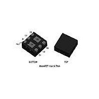
... Dimensional Outline and Pad Layout FDME1024NZT Rev.C1 6 www.fairchildsemi.com ...

Page 7

... Definition of Terms Datasheet Identification Product Status Advance Information Formative / In Design Preliminary First Production No Identification Needed Full Production Obsolete Not In Production FDME1024NZT Rev.C1 F-PFS™ Power-SPM™ ® FRFET PowerTrench SM Global Power Resource PowerXS™ Green FPS™ Programmable Active Droop™ ...

Related keywords