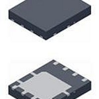
FDMS7660AS Fairchild Semiconductor, FDMS7660AS Datasheet - Page 4

FDMS7660AS
Manufacturer Part Number
FDMS7660AS
Description
MOSFET N-CH 30V PWRSTAGE POWER56
Manufacturer
Fairchild Semiconductor
Series
PowerTrench®, SyncFET™r
Datasheet
1.FDMS7660AS.pdf
(8 pages)
Specifications of FDMS7660AS
Fet Type
MOSFET N-Channel, Metal Oxide
Fet Feature
Logic Level Gate
Rds On (max) @ Id, Vgs
2.4 mOhm @ 25A, 10V
Drain To Source Voltage (vdss)
30V
Current - Continuous Drain (id) @ 25° C
26A
Vgs(th) (max) @ Id
3V @ 1mA
Gate Charge (qg) @ Vgs
90nC @ 10V
Input Capacitance (ciss) @ Vds
6120pF @ 15V
Power - Max
2.5W
Mounting Type
Surface Mount
Package / Case
8-PQFN, Power56
Configuration
Single
Transistor Polarity
N-Channel
Resistance Drain-source Rds (on)
2.5 m Ohms
Forward Transconductance Gfs (max / Min)
455 S
Drain-source Breakdown Voltage
30 V
Continuous Drain Current
42 A
Power Dissipation
83 W
Maximum Operating Temperature
+ 150 C
Mounting Style
SMD/SMT
Minimum Operating Temperature
- 55 C
Lead Free Status / RoHS Status
Lead free / RoHS Compliant
Available stocks
Company
Part Number
Manufacturer
Quantity
Price
Company:
Part Number:
FDMS7660AS
Manufacturer:
FAIRCHILD
Quantity:
579
Part Number:
FDMS7660AS
Manufacturer:
FAIRCHILD/仙童
Quantity:
20 000
FDMS7660AS Rev.C
Typical Characteristics
0.01
200
100
0.1
40
10
10
10
Figure 7.
8
6
4
2
0
1
0.01
1
0.01
0
I
THIS AREA IS
LIMITED BY r
D
Figure 9.
Figure 11. Forward Bias Safe
= 25 A
10
V
Switching Capability
SINGLE PULSE
T
R
T
V
DD
0.1
J
A
DS
Gate Charge Characteristics
θ
0.1
JA
= MAX RATED
t
= 25
AV
, DRAIN to SOURCE VOLTAGE (V)
Operating Area
= 10 V
Unclamped Inductive
= 125
20
DS(on)
, TIME IN AVALANCHE (ms)
Q
g
o
C
, GATE CHARGE (nC)
V
o
C/W
DD
30
T
= 15 V
J
1
1
= 125
T
J
= 25
40
V
T
o
DD
C
J
= 25 °C unless otherwise noted
o
= 20 V
C
10
T
10
50
J
= 100
o
60
100 ms
1 s
10 s
C
1 ms
10 ms
DC
100
100
300
70
200
4
1000
8000
1000
160
120
100
100
0.6
80
40
10
60
Figure 10.
0
1
10
0.1
25
Figure 12.
-3
f = 1 MHz
V
SINGLE PULSE
R
T
Figure 8.
GS
Current vs Case Temperature
A
θ
JA
Limited by Package
= 25
= 0 V
= 125
10
V
o
-2
50
DS
C
Power Dissipation
Maximum Continuous Drain
to Source Voltage
, DRAIN TO SOURCE VOLTAGE (V)
T
o
C/W
t, PULSE WIDTH (sec)
C
Single Pulse Maximum
Capacitance vs Drain
,
CASE TEMPERATURE (
10
-1
75
V
1
GS
= 4.5 V
1
R
100
V
θ
JC
GS
10
= 1.5
= 10 V
o
C )
o
C/W
125
V
www.fairchildsemi.com
10
100
GS
C
= 10 V
C
C
oss
rss
iss
1000
150
30


