S9S12XS128J1MAL Freescale Semiconductor, S9S12XS128J1MAL Datasheet - Page 116
S9S12XS128J1MAL
Manufacturer Part Number
S9S12XS128J1MAL
Description
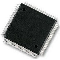
IC MCU 16BIT 128KB FLSH 112LQFP
Manufacturer
Freescale Semiconductor
Series
HCS12r
Datasheet
1.MC9S12XS64CAE.pdf
(738 pages)
Specifications of S9S12XS128J1MAL
Core Processor
HCS12X
Core Size
16-Bit
Speed
40MHz
Connectivity
CAN, SCI, SPI
Peripherals
LVD, POR, PWM, WDT
Number Of I /o
91
Program Memory Size
128KB (128K x 8)
Program Memory Type
FLASH
Eeprom Size
8K x 8
Ram Size
8K x 8
Voltage - Supply (vcc/vdd)
1.72 V ~ 5.5 V
Data Converters
A/D 16x12b
Oscillator Type
External
Operating Temperature
-40°C ~ 125°C
Package / Case
112-LQFP
Processor Series
S12XS
Core
HCS12
Data Bus Width
16 bit
Data Ram Size
8 KB
Interface Type
CAN, SCI, SPI
Maximum Clock Frequency
40 MHz
Number Of Programmable I/os
91
Number Of Timers
12
Maximum Operating Temperature
+ 125 C
Mounting Style
SMD/SMT
3rd Party Development Tools
EWHCS12
Development Tools By Supplier
DEMO9S12XSFAME, EVB9S12XEP100
Minimum Operating Temperature
- 40 C
On-chip Adc
12 bit, 16 Channel
Lead Free Status / RoHS Status
Lead free / RoHS Compliant
Available stocks
Company
Part Number
Manufacturer
Quantity
Price
Company:

Part Number:
S9S12XS128J1MAL
Manufacturer:
Freescale Semiconductor
Quantity:
10 000


1
1
Port Integration Module (S12XSPIMV1)
2.3.65
2.3.66
116
Function
Address 0x026F
Address 0x0270
PT0AD0
7-6, 1-0
Read: Anytime.
Write: Anytime.
Read: Anytime. The data source depends on the data direction value.
Write: Anytime.
Altern.
Field
Field
PIFJ
Reset
Reset
7-0
W
W
R
R
PT0AD07
Port J interrupt flag—
The flag bit is set after an active edge was applied to the associated input pin. This can be a rising or a falling edge
based on the state of the polarity select register.
Writing a logic “1” to the corresponding bit field clears the flag.
1 Active edge on the associated bit has occurred (an interrupt will occur if the associated enable bit is set)
0 No active edge occurred
Port AD0 general purpose input/output data—Data Register, ATD AN analog input
When not used with the alternative function, the associated pin can be used as general purpose I/O. In general
purpose output mode the register bit value is driven to the pin.
If the associated data direction bit is set to 1, a read returns the value of the port register bit, otherwise the buffered
pin input state is read.
PIFJ7
AN15
Port J Interrupt Flag Register (PIFJ)
Port AD0 Data Register 0 (PT0AD0)
0
0
7
7
PT0AD06
PIFJ6
AN14
0
0
6
6
Figure 2-63. Port J Interrupt Flag Register (PIFJ)
Figure 2-64. Port AD0 Data Register 0 (PT0AD0)
Table 2-63. PT0AD0 Register Field Descriptions
Table 2-62. PIFJ Register Field Descriptions
S12XS Family Reference Manual, Rev. 1.11
PT0AD05
AN13
0
0
0
5
5
PT0AD04
AN12
0
0
0
4
4
Description
Description
PT0AD03
AN11
3
0
0
3
0
PT0AD02
AN10
0
0
0
2
2
PT0AD01
Freescale Semiconductor
Access: User read/write
Access: User read/write
PIFJ1
AN9
0
0
1
1
PT0AD00
PIFJ0
AN8
0
0
0
0
1
1
Related parts for S9S12XS128J1MAL
Image
Part Number
Description
Manufacturer
Datasheet
Request
R

Part Number:
Description:
Manufacturer:
Freescale Semiconductor, Inc
Datasheet:
Part Number:
Description:
Manufacturer:
Freescale Semiconductor, Inc
Datasheet:
Part Number:
Description:
Manufacturer:
Freescale Semiconductor, Inc
Datasheet:
Part Number:
Description:
Manufacturer:
Freescale Semiconductor, Inc
Datasheet:
Part Number:
Description:
Manufacturer:
Freescale Semiconductor, Inc
Datasheet:
Part Number:
Description:
Manufacturer:
Freescale Semiconductor, Inc
Datasheet:
Part Number:
Description:
Manufacturer:
Freescale Semiconductor, Inc
Datasheet:
Part Number:
Description:
Manufacturer:
Freescale Semiconductor, Inc
Datasheet:
Part Number:
Description:
Manufacturer:
Freescale Semiconductor, Inc
Datasheet:
Part Number:
Description:
Manufacturer:
Freescale Semiconductor, Inc
Datasheet:
Part Number:
Description:
Manufacturer:
Freescale Semiconductor, Inc
Datasheet:
Part Number:
Description:
Manufacturer:
Freescale Semiconductor, Inc
Datasheet:
Part Number:
Description:
Manufacturer:
Freescale Semiconductor, Inc
Datasheet:
Part Number:
Description:
Manufacturer:
Freescale Semiconductor, Inc
Datasheet:
Part Number:
Description:
Manufacturer:
Freescale Semiconductor, Inc
Datasheet: