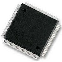
S9S12XS128J1MAL Freescale Semiconductor, S9S12XS128J1MAL Datasheet - Page 128

S9S12XS128J1MAL
Manufacturer Part Number
S9S12XS128J1MAL
Description
IC MCU 16BIT 128KB FLSH 112LQFP
Manufacturer
Freescale Semiconductor
Series
HCS12r
Datasheet
1.MC9S12XS64CAE.pdf
(738 pages)
Specifications of S9S12XS128J1MAL
Core Processor
HCS12X
Core Size
16-Bit
Speed
40MHz
Connectivity
CAN, SCI, SPI
Peripherals
LVD, POR, PWM, WDT
Number Of I /o
91
Program Memory Size
128KB (128K x 8)
Program Memory Type
FLASH
Eeprom Size
8K x 8
Ram Size
8K x 8
Voltage - Supply (vcc/vdd)
1.72 V ~ 5.5 V
Data Converters
A/D 16x12b
Oscillator Type
External
Operating Temperature
-40°C ~ 125°C
Package / Case
112-LQFP
Processor Series
S12XS
Core
HCS12
Data Bus Width
16 bit
Data Ram Size
8 KB
Interface Type
CAN, SCI, SPI
Maximum Clock Frequency
40 MHz
Number Of Programmable I/os
91
Number Of Timers
12
Maximum Operating Temperature
+ 125 C
Mounting Style
SMD/SMT
3rd Party Development Tools
EWHCS12
Development Tools By Supplier
DEMO9S12XSFAME, EVB9S12XEP100
Minimum Operating Temperature
- 40 C
On-chip Adc
12 bit, 16 Channel
Lead Free Status / RoHS Status
Lead free / RoHS Compliant
Available stocks
Company
Part Number
Manufacturer
Quantity
Price
Company:
Part Number:
S9S12XS128J1MAL
Manufacturer:
Freescale Semiconductor
Quantity:
10 000
- Current page: 128 of 738
- Download datasheet (4Mb)
Memory Mapping Control (S12XMMCV4)
3.1.1
3.1.2
The main features of this block are:
1.
128
Resources are also called targets.
•
•
•
•
•
•
•
•
•
Unimplemented areas
Mis-aligned address
single-chip modes
Paging capability to support a global 8MB memory address space
Bus arbitration between the masters CPU, BDM
Simultaneous accesses to different resources
Resolution of target bus access collision
MCU operation mode control
MCU security control
Separate memory map schemes for each master CPU, BDM
ROM control bits to enable the on-chip FLASH or ROM selection
Generation of system reset when CPU accesses an unimplemented address (i.e., an address which
does not belong to any of the on-chip modules) in single-chip modes
Aligned address
global address
normal modes
special modes
Logic level “1”
Logic level “0”
local address
Bus Clock
Terminology
Features
MCU
NVM
word
PRR
PRU
Byte
IFR
NS
SS
0x
x
Voltage that corresponds to Boolean true state
Voltage that corresponds to Boolean false state
Represents hexadecimal number
Represents logic level ’don’t care’
8-bit data
16-bit data
based on the 64KB Memory Space (16-bit address)
based on the 8MB Memory Space (23-bit address)
Address on even boundary
Address on odd boundary
System Clock. Refer to CRG Block Guide.
Normal Single-Chip Mode
Special Single-Chip Mode
Normal Single-Chip Mode
Special Single-Chip Mode
Normal Single-Chip Mode
Special Single-Chip Mode
Areas which are accessible by the pages (RPAGE,PPAGE,EPAGE) and not implemented
Port Replacement Registers
Port Replacement Unit located on the emulator side
MicroController Unit
Non-volatile Memory; Flash, Data FLASH or ROM
Information Row sector located on the top of NVM. For Test purposes.
Table 3-1. Acronyms and Abbreviations
S12XS Family Reference Manual, Rev. 1.11
1
(internal, and peripherals) (see
Freescale Semiconductor
Figure 3-1
)
Related parts for S9S12XS128J1MAL
Image
Part Number
Description
Manufacturer
Datasheet
Request
R
Part Number:
Description:
Manufacturer:
Freescale Semiconductor, Inc
Datasheet:
Part Number:
Description:
Manufacturer:
Freescale Semiconductor, Inc
Datasheet:
Part Number:
Description:
Manufacturer:
Freescale Semiconductor, Inc
Datasheet:
Part Number:
Description:
Manufacturer:
Freescale Semiconductor, Inc
Datasheet:
Part Number:
Description:
Manufacturer:
Freescale Semiconductor, Inc
Datasheet:
Part Number:
Description:
Manufacturer:
Freescale Semiconductor, Inc
Datasheet:
Part Number:
Description:
Manufacturer:
Freescale Semiconductor, Inc
Datasheet:
Part Number:
Description:
Manufacturer:
Freescale Semiconductor, Inc
Datasheet:
Part Number:
Description:
Manufacturer:
Freescale Semiconductor, Inc
Datasheet:
Part Number:
Description:
Manufacturer:
Freescale Semiconductor, Inc
Datasheet:
Part Number:
Description:
Manufacturer:
Freescale Semiconductor, Inc
Datasheet:
Part Number:
Description:
Manufacturer:
Freescale Semiconductor, Inc
Datasheet:
Part Number:
Description:
Manufacturer:
Freescale Semiconductor, Inc
Datasheet:
Part Number:
Description:
Manufacturer:
Freescale Semiconductor, Inc
Datasheet:
Part Number:
Description:
Manufacturer:
Freescale Semiconductor, Inc
Datasheet:


