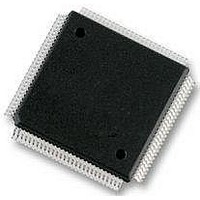
S9S12XS128J1MAL Freescale Semiconductor, S9S12XS128J1MAL Datasheet - Page 373

S9S12XS128J1MAL
Manufacturer Part Number
S9S12XS128J1MAL
Description
IC MCU 16BIT 128KB FLSH 112LQFP
Manufacturer
Freescale Semiconductor
Series
HCS12r
Datasheet
1.MC9S12XS64CAE.pdf
(738 pages)
Specifications of S9S12XS128J1MAL
Core Processor
HCS12X
Core Size
16-Bit
Speed
40MHz
Connectivity
CAN, SCI, SPI
Peripherals
LVD, POR, PWM, WDT
Number Of I /o
91
Program Memory Size
128KB (128K x 8)
Program Memory Type
FLASH
Eeprom Size
8K x 8
Ram Size
8K x 8
Voltage - Supply (vcc/vdd)
1.72 V ~ 5.5 V
Data Converters
A/D 16x12b
Oscillator Type
External
Operating Temperature
-40°C ~ 125°C
Package / Case
112-LQFP
Processor Series
S12XS
Core
HCS12
Data Bus Width
16 bit
Data Ram Size
8 KB
Interface Type
CAN, SCI, SPI
Maximum Clock Frequency
40 MHz
Number Of Programmable I/os
91
Number Of Timers
12
Maximum Operating Temperature
+ 125 C
Mounting Style
SMD/SMT
3rd Party Development Tools
EWHCS12
Development Tools By Supplier
DEMO9S12XSFAME, EVB9S12XEP100
Minimum Operating Temperature
- 40 C
On-chip Adc
12 bit, 16 Channel
Lead Free Status / RoHS Status
Lead free / RoHS Compliant
Available stocks
Company
Part Number
Manufacturer
Quantity
Price
Company:
Part Number:
S9S12XS128J1MAL
Manufacturer:
Freescale Semiconductor
Quantity:
10 000
- Current page: 373 of 738
- Download datasheet (4Mb)
Read: Anytime
Write: Anytime
13.3.2.4
This register selects the prescale clock source for clocks A and B independently.
Freescale Semiconductor
Module Base + 0x0002
Reset
PCLK7
PCLK6
PCLK5
PCLK4
PCLK3
PCLK2
PCLK1
PCLK0
Field
7
6
5
4
3
2
1
0
W
R
PCLK7
Pulse Width Channel 7 Clock Select
0 Clock B is the clock source for PWM channel 7.
1 Clock SB is the clock source for PWM channel 7.
Pulse Width Channel 6 Clock Select
0 Clock B is the clock source for PWM channel 6.
1 Clock SB is the clock source for PWM channel 6.
Pulse Width Channel 5 Clock Select
0 Clock A is the clock source for PWM channel 5.
1 Clock SA is the clock source for PWM channel 5.
Pulse Width Channel 4 Clock Select
0 Clock A is the clock source for PWM channel 4.
1 Clock SA is the clock source for PWM channel 4.
Pulse Width Channel 3 Clock Select
0 Clock B is the clock source for PWM channel 3.
1 Clock SB is the clock source for PWM channel 3.
Pulse Width Channel 2 Clock Select
0 Clock B is the clock source for PWM channel 2.
1 Clock SB is the clock source for PWM channel 2.
Pulse Width Channel 1 Clock Select
0 Clock A is the clock source for PWM channel 1.
1 Clock SA is the clock source for PWM channel 1.
Pulse Width Channel 0 Clock Select
0 Clock A is the clock source for PWM channel 0.
1 Clock SA is the clock source for PWM channel 0.
PWM Prescale Clock Select Register (PWMPRCLK)
0
7
Register bits PCLK0 to PCLK7 can be written anytime. If a clock select is
changed while a PWM signal is being generated, a truncated or stretched
pulse can occur during the transition.
PCLKL6
0
6
Figure 13-5. PWM Clock Select Register (PWMCLK)
Table 13-3. PWMCLK Field Descriptions
S12XS Family Reference Manual, Rev. 1.11
PCLK5
0
5
PCLK4
NOTE
0
4
Description
PCLK3
0
3
Pulse-Width Modulator (S12PWM8B8CV1)
PCLK2
0
2
PCLK1
0
1
PCLK0
0
0
373
Related parts for S9S12XS128J1MAL
Image
Part Number
Description
Manufacturer
Datasheet
Request
R
Part Number:
Description:
Manufacturer:
Freescale Semiconductor, Inc
Datasheet:
Part Number:
Description:
Manufacturer:
Freescale Semiconductor, Inc
Datasheet:
Part Number:
Description:
Manufacturer:
Freescale Semiconductor, Inc
Datasheet:
Part Number:
Description:
Manufacturer:
Freescale Semiconductor, Inc
Datasheet:
Part Number:
Description:
Manufacturer:
Freescale Semiconductor, Inc
Datasheet:
Part Number:
Description:
Manufacturer:
Freescale Semiconductor, Inc
Datasheet:
Part Number:
Description:
Manufacturer:
Freescale Semiconductor, Inc
Datasheet:
Part Number:
Description:
Manufacturer:
Freescale Semiconductor, Inc
Datasheet:
Part Number:
Description:
Manufacturer:
Freescale Semiconductor, Inc
Datasheet:
Part Number:
Description:
Manufacturer:
Freescale Semiconductor, Inc
Datasheet:
Part Number:
Description:
Manufacturer:
Freescale Semiconductor, Inc
Datasheet:
Part Number:
Description:
Manufacturer:
Freescale Semiconductor, Inc
Datasheet:
Part Number:
Description:
Manufacturer:
Freescale Semiconductor, Inc
Datasheet:
Part Number:
Description:
Manufacturer:
Freescale Semiconductor, Inc
Datasheet:
Part Number:
Description:
Manufacturer:
Freescale Semiconductor, Inc
Datasheet:


