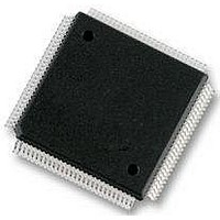
S9S12XS128J1MAL Freescale Semiconductor, S9S12XS128J1MAL Datasheet - Page 223

S9S12XS128J1MAL
Manufacturer Part Number
S9S12XS128J1MAL
Description
IC MCU 16BIT 128KB FLSH 112LQFP
Manufacturer
Freescale Semiconductor
Series
HCS12r
Datasheet
1.MC9S12XS64CAE.pdf
(738 pages)
Specifications of S9S12XS128J1MAL
Core Processor
HCS12X
Core Size
16-Bit
Speed
40MHz
Connectivity
CAN, SCI, SPI
Peripherals
LVD, POR, PWM, WDT
Number Of I /o
91
Program Memory Size
128KB (128K x 8)
Program Memory Type
FLASH
Eeprom Size
8K x 8
Ram Size
8K x 8
Voltage - Supply (vcc/vdd)
1.72 V ~ 5.5 V
Data Converters
A/D 16x12b
Oscillator Type
External
Operating Temperature
-40°C ~ 125°C
Package / Case
112-LQFP
Processor Series
S12XS
Core
HCS12
Data Bus Width
16 bit
Data Ram Size
8 KB
Interface Type
CAN, SCI, SPI
Maximum Clock Frequency
40 MHz
Number Of Programmable I/os
91
Number Of Timers
12
Maximum Operating Temperature
+ 125 C
Mounting Style
SMD/SMT
3rd Party Development Tools
EWHCS12
Development Tools By Supplier
DEMO9S12XSFAME, EVB9S12XEP100
Minimum Operating Temperature
- 40 C
On-chip Adc
12 bit, 16 Channel
Lead Free Status / RoHS Status
Lead free / RoHS Compliant
Available stocks
Company
Part Number
Manufacturer
Quantity
Price
Company:
Part Number:
S9S12XS128J1MAL
Manufacturer:
Freescale Semiconductor
Quantity:
10 000
- Current page: 223 of 738
- Download datasheet (4Mb)
6.4.5.3
Referring to
INF bytes contain control information (R/W, S/D etc.). The numerical suffix indicates which tracing step.
The information format for Loop1 Mode and PurePC Mode is the same as that of Normal Mode. Whilst
tracing in Normal or Loop1 modes each array line contains 2 data entries, thus in this case the DBGCNT[0]
is incremented after each separate entry. In Detail mode DBGCNT[0] remains cleared whilst the other
DBGCNT bits are incremented on each trace buffer entry.
When a COF occurs a trace buffer entry is made and the corresponding CDV bit is set.
Single byte data accesses in Detail Mode are always stored to the low byte of the trace buffer (CDATAL )
and the high byte is cleared. When tracing word accesses, the byte at the lower address is always stored to
trace buffer byte3 and the byte at the higher address is stored to byte2
Freescale Semiconductor
Other Modes
S12XCPU
CPU12X
Mode
Detail
Table
Trace Buffer Organization
CXINF1
CXINF2
CINF1
CINF3
6-40. ADRH, ADRM, ADRL denote address high, middle and low byte respectively.
7
CADRH1
CADRH2
CPCH1
CPCH3
6
S12XS Family Reference Manual, Rev. 1.11
Table 6-40. Trace Buffer Organization
CADRM1
CADRM2
CPCM1
CPCM3
5
8-Byte Wide Word Buffer
CADRL1
CADRL2
CPCL1
CPCL3
4
CDATAH1
CDATAH2
CINF0
CINF2
3
CDATAL1
CDATAL2
CPCH0
CPCH2
2
S12X Debug (S12XDBGV3) Module
CPCM0
CPCM2
1
CPCL0
CPCL2
0
223
Related parts for S9S12XS128J1MAL
Image
Part Number
Description
Manufacturer
Datasheet
Request
R
Part Number:
Description:
Manufacturer:
Freescale Semiconductor, Inc
Datasheet:
Part Number:
Description:
Manufacturer:
Freescale Semiconductor, Inc
Datasheet:
Part Number:
Description:
Manufacturer:
Freescale Semiconductor, Inc
Datasheet:
Part Number:
Description:
Manufacturer:
Freescale Semiconductor, Inc
Datasheet:
Part Number:
Description:
Manufacturer:
Freescale Semiconductor, Inc
Datasheet:
Part Number:
Description:
Manufacturer:
Freescale Semiconductor, Inc
Datasheet:
Part Number:
Description:
Manufacturer:
Freescale Semiconductor, Inc
Datasheet:
Part Number:
Description:
Manufacturer:
Freescale Semiconductor, Inc
Datasheet:
Part Number:
Description:
Manufacturer:
Freescale Semiconductor, Inc
Datasheet:
Part Number:
Description:
Manufacturer:
Freescale Semiconductor, Inc
Datasheet:
Part Number:
Description:
Manufacturer:
Freescale Semiconductor, Inc
Datasheet:
Part Number:
Description:
Manufacturer:
Freescale Semiconductor, Inc
Datasheet:
Part Number:
Description:
Manufacturer:
Freescale Semiconductor, Inc
Datasheet:
Part Number:
Description:
Manufacturer:
Freescale Semiconductor, Inc
Datasheet:
Part Number:
Description:
Manufacturer:
Freescale Semiconductor, Inc
Datasheet:


