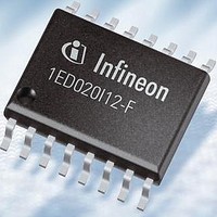
1ED020I12-F Infineon Technologies, 1ED020I12-F Datasheet - Page 10

1ED020I12-F
Manufacturer Part Number
1ED020I12-F
Description
MOSFET & Power Driver ICs SNGL IGBT Driver IC IGBT Driver IC
Manufacturer
Infineon Technologies
Datasheet
1.1ED020I12-F.pdf
(22 pages)
Specifications of 1ED020I12-F
Product
Driver ICs - Various
Rise Time
400 ns
Fall Time
600 ns
Supply Voltage (max)
5.5 V, 20 V, 0 V
Supply Voltage (min)
4.5 V, 13 V, - 12 V
Maximum Power Dissipation
700 mW
Maximum Operating Temperature
+ 105 C
Mounting Style
SMD/SMT
Minimum Operating Temperature
- 40 C
Number Of Drivers
1
Number Of Outputs
1
Package / Case
PG-DSO-16-15
Lead Free Status / RoHS Status
Lead free / RoHS Compliant
Available stocks
Company
Part Number
Manufacturer
Quantity
Price
Company:
Part Number:
1ED020I12-F
Manufacturer:
VISHAY
Quantity:
400 000
Part Number:
1ED020I12-F
Manufacturer:
INFINEON/英飞凌
Quantity:
20 000
Company:
Part Number:
1ED020I12-F2
Manufacturer:
INFINEON
Quantity:
2 190
Part Number:
1ED020I12-F2
Manufacturer:
INFINEON/英飞凌
Quantity:
20 000
Part Number:
1ED020I12-FA
Manufacturer:
INFINEON/英飞凌
Quantity:
20 000
Part Number:
1ED020I12-FT
Manufacturer:
INFINEON/英飞凌
Quantity:
20 000
4
4.1
Note: Absolute maximum ratings are defined as ratings, which when being exceeded may lead to destruction of the integrated
Parameter
Positive power supply output side
Negative power supply output side
Maximum power supply voltage output side
(V
Gate driver output
Gate driver high output maximum current
Gate driver low output maximum current
Maximum short circuit clamping time
Positive power supply input side
Logic input voltages
(IN+,IN-,RST)
Opendrain Logic output voltage
(FLT)
Opendrain Logic output voltage
(RDY)
Opendrain Logic output current
(FAULT)
Opendrain Logic output current
(RDY)
Pin DESAT voltage
Pin CLAMP voltage
Junction temperature
Storage temperature
Power dissipation, Input chip
Power dissipation, Output chip
Thermal resistance (Input chip active)
Thermal resistance (Output chip active)
ESD Capability
1) With respect to GND2.
2) may be exceeded during short circuit clamping
3) Output IC power dissipation is derated linearly at 10 mW/°C above 62°C. Input IC power dissipation does not require derating. See
4) According to EIA/JESD22-A114-B (discharging a 100pF capacitor through a 1.5k series resistor).
Datasheet
VCC2
section 8.1 for reference layouts for these thermal data. Thermal performance may change significantly with layout and heat dissipation
of components in close proximity.
circuit. Unless otherwise noted all parameters refer to GND1.
-V
VEE2
)
Electrical Parameters
Absolute Maximum Ratings
Symbol
V
V
V
V
I
I
t
V
V
V
V
I
I
V
V
T
T
P
P
R
R
V
CLP
OUT
OUT
FLT
RDY
D, IN
D, OUT
J
S
THJA,IN
THJA,OUT
VCC2
VEE2
max2
OUT
VCC1
LogicIN
FLT
RDY
DESAT
CLAMP
ESD
10
V
V
VEE2
VEE2
min.
-0.3
-0.3
-0.3
-0.3
-0.3
-0.3
-12
-40
-55
—
—
Limit Values
-0.3 V
-0.3 V
2)
V
max2
VCC2
VCC2
max.
150
150
100
700
160
125
0.3
2.4
2.4
6.5
6.5
6.5
6.5
20
28
10
10
10
1
+0.3
+0.3
+0.3
Unit Remarks
K/W @TA = 25°C
K/W @TA = 25°C
mW
mW
mA
mA
kV
°C
°C
us
V
V
V
V
A
A
V
V
V
V
V
V
Version 2.2, 2009-12-03
Electrical Parameters
EICEDRIVER
1)
1)
t = 2µs
t = 2µs
I
500mA
1)
3)
3)
Human Body
Model
CLAMP/OUT
@TA = 25°
@TA = 25°
V
1ED020I12-F
VEE2
4)
= -8V
=
TM


