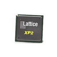
LFXP2-8E-5FTN256C Lattice, LFXP2-8E-5FTN256C Datasheet - Page 107

LFXP2-8E-5FTN256C
Manufacturer Part Number
LFXP2-8E-5FTN256C
Description
FPGA - Field Programmable Gate Array 8K LUTs 201I/O Inst- on DSP 1.2V -5 Spd
Manufacturer
Lattice
Datasheet
1.LFXP2-8E-5FTN256I.pdf
(341 pages)
Specifications of LFXP2-8E-5FTN256C
Number Of Macrocells
8000
Number Of Programmable I/os
201
Data Ram Size
226304
Supply Voltage (max)
1.26 V
Maximum Operating Temperature
+ 85 C
Minimum Operating Temperature
0 C
Mounting Style
SMD/SMT
Supply Voltage (min)
1.14 V
Package / Case
FTBGA-256
Lead Free Status / RoHS Status
Lead free / RoHS Compliant
Available stocks
Company
Part Number
Manufacturer
Quantity
Price
Company:
Part Number:
LFXP2-8E-5FTN256C
Manufacturer:
Lattice
Quantity:
63
Company:
Part Number:
LFXP2-8E-5FTN256C
Manufacturer:
Lattice Semiconductor Corporation
Quantity:
10 000
- Current page: 107 of 341
- Download datasheet (10Mb)
Lattice Semiconductor
Table 8-2. Supported Output Standards (Continued)
sysIO Banking Scheme
LatticeXP2 devices have eight general purpose programmable sysIO banks. Each of the eight general purpose
sysIO banks has a V
general purpose banks.
On the top and bottom banks, the sysIO buffer pair consists of two single-ended output drivers and two sets of sin-
gle-ended input buffers (both ratioed and referenced). The left and right sysIO buffer pair consists of two single-
ended output drivers and two sets of single-ended input buffers (both ratioed and referenced). The referenced input
buffer can also be configured as a differential input. True LVDS support is available on only 50% of the left and right
I/Os (starting with the topmost pairs). There are no LVDS on the top and bottom I/Os. In 50% of the pairs there is
also one differential output driver. The two pads in the pair are described as “true” and “comp”, where the true pad
is associated with the positive side of the differential input buffer and the comp (complementary) pad is associated
with the negative side of the differential input buffer.
SPI Flash Interface
The SPI pins (master/slave) are multiplexed with the I/Os in Bank 7. The two dedicated pins CFG[0] and TOE are
powered by V
JTAG Interface
The JTAG pins are located between Banks 2 and 3 and are powered by V
Figure 8-1. LatticeXP2 sysIO Banking
LVDS
MLVDS
BLVDS
LVPECL
RSDS
1. Emulated with external resistors.
2. PCI33 is PCIX compatible.
1
1
1
1
Output Standard
CC
and reside between Banks 6 and 7.
CCIO
supply voltage, and two reference voltages, V
Bank 6
Bank 7
Bank 0
Bank 5
Drive
N/A
N/A
N/A
N/A
N/A
8-3
Bank 1
Bank 4
REF1
CCJ
LatticeXP2 sysIO Usage Guide
and V
Bank 2
Bank 3
.
REF2
. Figure 8-1 shows the eight
V
CCIO
2.5
2.5
2.5
3.3
2.5
(Nom.)
Related parts for LFXP2-8E-5FTN256C
Image
Part Number
Description
Manufacturer
Datasheet
Request
R

Part Number:
Description:
FPGA - Field Programmable Gate Array 8K LUTs 100I/O Inst- on DSP 1.2V -5 Spd
Manufacturer:
Lattice
Datasheet:

Part Number:
Description:
FPGA - Field Programmable Gate Array 8K LUTs 201 I/O Inst on DSP 1.2V -5 Spd
Manufacturer:
Lattice
Datasheet:

Part Number:
Description:
FPGA - Field Programmable Gate Array 8K LUTs 100 I/O Inst on DSP 1.2V -5 Spd
Manufacturer:
Lattice
Datasheet:

Part Number:
Description:
IC, LATTICEXP2 FPGA, 435MHZ, QFP-208
Manufacturer:
LATTICE SEMICONDUCTOR
Datasheet:

Part Number:
Description:
FPGA - Field Programmable Gate Array 8K LUTs 86I/O Inst- on DSP 1.2V -5 Spd
Manufacturer:
Lattice

Part Number:
Description:
FPGA - Field Programmable Gate Array 8K LUTs 201I/O Inst- on DSP 1.2V -7 Spd
Manufacturer:
Lattice
Datasheet:
Part Number:
Description:
FPGA LatticeXP2 Family 8000 Cells Flash Technology 1.2V 144-Pin TQFP
Manufacturer:
LATTICE SEMICONDUCTOR
Datasheet:

Part Number:
Description:
IC DSP 8KLUTS 146I/O 208PQFP
Manufacturer:
Lattice
Datasheet:

Part Number:
Description:
IC DSP 8KLUTS 100I/O 144TQFP
Manufacturer:
Lattice
Datasheet:

Part Number:
Description:
IC DSP 8KLUTS 86I/O 132CSBGA
Manufacturer:
Lattice
Datasheet:

Part Number:
Description:
IC DSP 8KLUTS 86I/O 132CSBGA
Manufacturer:
Lattice
Datasheet:

Part Number:
Description:
IC DSP 8KLUTS 146I/O 208PQFP
Manufacturer:
Lattice
Datasheet:

Part Number:
Description:
IC DSP 8KLUTS 201I/O 256FTBGA
Manufacturer:
Lattice
Datasheet:

Part Number:
Description:
IC FPGA 8KLUTS 86I/O 132-BGA
Manufacturer:
Lattice
Datasheet:

Part Number:
Description:
IC FPGA 8KLUTS 86I/O 132-BGA
Manufacturer:
Lattice
Datasheet:


