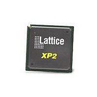
LFXP2-8E-5FTN256C Lattice, LFXP2-8E-5FTN256C Datasheet - Page 127

LFXP2-8E-5FTN256C
Manufacturer Part Number
LFXP2-8E-5FTN256C
Description
FPGA - Field Programmable Gate Array 8K LUTs 201I/O Inst- on DSP 1.2V -5 Spd
Manufacturer
Lattice
Datasheet
1.LFXP2-8E-5FTN256I.pdf
(341 pages)
Specifications of LFXP2-8E-5FTN256C
Number Of Macrocells
8000
Number Of Programmable I/os
201
Data Ram Size
226304
Supply Voltage (max)
1.26 V
Maximum Operating Temperature
+ 85 C
Minimum Operating Temperature
0 C
Mounting Style
SMD/SMT
Supply Voltage (min)
1.14 V
Package / Case
FTBGA-256
Lead Free Status / RoHS Status
Lead free / RoHS Compliant
Available stocks
Company
Part Number
Manufacturer
Quantity
Price
Company:
Part Number:
LFXP2-8E-5FTN256C
Manufacturer:
Lattice
Quantity:
63
Company:
Part Number:
LFXP2-8E-5FTN256C
Manufacturer:
Lattice Semiconductor Corporation
Quantity:
10 000
- Current page: 127 of 341
- Download datasheet (10Mb)
LatticeXP2 sysCLOCK PLL
Lattice Semiconductor
Design and Usage Guide
Functional Description
PLL Divider and Delay Blocks
Input Clock (CLKI) Divider
The CLKI divider is used to control the input clock frequency into the PLL block. The divider setting directly corre-
sponds to the divisor of the output clock. The input and output of the input divider must be within the input and out-
put frequency ranges specified in the device data sheet.
Feedback Loop (CLKFB) Divider
The CLKFB divider is used to divide the feedback signal. Effectively, this multiplies the output clock, because the
divided feedback must speed up to match the input frequency into the PLL block. The PLL block increases the out-
put frequency until the divided feedback frequency equals the input frequency. The input and output of the feed-
back divider must be within the input and output frequency ranges specified in the device data sheet.
Output Clock (CLKOP) Divider
The CLKOP divider serves the dual purposes of squaring the duty cycle of the VCO output and scaling up the VCO
frequency into the 435MHz to 870MHz range to minimize jitter. The CLKOP divider values are the same whether or
not the CLKOS is used.
CLKOK Divider
The CLKOK divider acts as a source for the global clock nets. It divides the CLKOP signal of the PLL by the value
of the divider to produce lower frequency clock.
CLKOK2 Divider
The CLKOK2 is CLKOP divided by 3 for generating 140 MHz from 420 MHz to support SPI4.2.
Phase Adjustment and Duty Cycle Select (Static Mode)
Users can program CLKOS with Phase and Duty Cycle options. Phase adjustment can be done in 22.5° steps. The
duty cycle resolution is 1/16th of a period except 1/16th and 15/16th duty cycle options are not supported to avoid
minimum pulse violation.
Dynamic Phase Adjustment (DPHASE) and Dynamic Duty Cycle (DDUTY) Select
The Phase Adjustment and Duty Cycle Select can be controlled in dynamic mode. When this mode is selected,
both the Phase Adjustment and Duty Cycle Select must be in dynamic mode. If only one of the features is to be
used in dynamic mode, users can set the other control inputs with the fixed logic levels of their choice.
Duty Trim Adjustment
With the LatticeXP2 device family, the duty cycle can be fine-tuned with the Duty Trim Adjustment.
Fine Delay Adjust
This optional feature is controlled by the input port, WRDEL. See information on the WRDEL input in the next sec-
tion of this document.
PLL Inputs and Outputs
CLKI Input
The CLKI signal is the reference clock for the PLL. It must conform to the specifications in the data sheet in order
for the PLL to operate correctly. The CLKI can be derived from a dedicated dual-purpose pin or from routing.
RST Input
The PLL reset occurs under two conditions. At power-up an internal power-up reset signal from the configuration
block resets the PLL. The user-controlled PLL reset signal RST is provided as part of the PLL module that can be
driven by an internally generated reset function or a pin. This RST signal resets all internal PLL counters, flip-flops
(including the M-Divider) and the charge pump. The M-Divider reset synchronizes the M-Divider output to the input
clock. When RST goes inactive, the PLL will start the lock-in process, and will take the t
time to complete the
LOCK
PLL lock. Figure 9-5 shows the timing diagram of the RST input. RST is active high. The RST signal is optional.
9-5
Related parts for LFXP2-8E-5FTN256C
Image
Part Number
Description
Manufacturer
Datasheet
Request
R

Part Number:
Description:
FPGA - Field Programmable Gate Array 8K LUTs 100I/O Inst- on DSP 1.2V -5 Spd
Manufacturer:
Lattice
Datasheet:

Part Number:
Description:
FPGA - Field Programmable Gate Array 8K LUTs 201 I/O Inst on DSP 1.2V -5 Spd
Manufacturer:
Lattice
Datasheet:

Part Number:
Description:
FPGA - Field Programmable Gate Array 8K LUTs 100 I/O Inst on DSP 1.2V -5 Spd
Manufacturer:
Lattice
Datasheet:

Part Number:
Description:
IC, LATTICEXP2 FPGA, 435MHZ, QFP-208
Manufacturer:
LATTICE SEMICONDUCTOR
Datasheet:

Part Number:
Description:
FPGA - Field Programmable Gate Array 8K LUTs 86I/O Inst- on DSP 1.2V -5 Spd
Manufacturer:
Lattice

Part Number:
Description:
FPGA - Field Programmable Gate Array 8K LUTs 201I/O Inst- on DSP 1.2V -7 Spd
Manufacturer:
Lattice
Datasheet:
Part Number:
Description:
FPGA LatticeXP2 Family 8000 Cells Flash Technology 1.2V 144-Pin TQFP
Manufacturer:
LATTICE SEMICONDUCTOR
Datasheet:

Part Number:
Description:
IC DSP 8KLUTS 146I/O 208PQFP
Manufacturer:
Lattice
Datasheet:

Part Number:
Description:
IC DSP 8KLUTS 100I/O 144TQFP
Manufacturer:
Lattice
Datasheet:

Part Number:
Description:
IC DSP 8KLUTS 86I/O 132CSBGA
Manufacturer:
Lattice
Datasheet:

Part Number:
Description:
IC DSP 8KLUTS 86I/O 132CSBGA
Manufacturer:
Lattice
Datasheet:

Part Number:
Description:
IC DSP 8KLUTS 146I/O 208PQFP
Manufacturer:
Lattice
Datasheet:

Part Number:
Description:
IC DSP 8KLUTS 201I/O 256FTBGA
Manufacturer:
Lattice
Datasheet:

Part Number:
Description:
IC FPGA 8KLUTS 86I/O 132-BGA
Manufacturer:
Lattice
Datasheet:

Part Number:
Description:
IC FPGA 8KLUTS 86I/O 132-BGA
Manufacturer:
Lattice
Datasheet:


