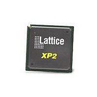
LFXP2-8E-5FTN256C Lattice, LFXP2-8E-5FTN256C Datasheet - Page 289

LFXP2-8E-5FTN256C
Manufacturer Part Number
LFXP2-8E-5FTN256C
Description
FPGA - Field Programmable Gate Array 8K LUTs 201I/O Inst- on DSP 1.2V -5 Spd
Manufacturer
Lattice
Datasheet
1.LFXP2-8E-5FTN256I.pdf
(341 pages)
Specifications of LFXP2-8E-5FTN256C
Number Of Macrocells
8000
Number Of Programmable I/os
201
Data Ram Size
226304
Supply Voltage (max)
1.26 V
Maximum Operating Temperature
+ 85 C
Minimum Operating Temperature
0 C
Mounting Style
SMD/SMT
Supply Voltage (min)
1.14 V
Package / Case
FTBGA-256
Lead Free Status / RoHS Status
Lead free / RoHS Compliant
Available stocks
Company
Part Number
Manufacturer
Quantity
Price
Company:
Part Number:
LFXP2-8E-5FTN256C
Manufacturer:
Lattice
Quantity:
63
Company:
Part Number:
LFXP2-8E-5FTN256C
Manufacturer:
Lattice Semiconductor Corporation
Quantity:
10 000
- Current page: 289 of 341
- Download datasheet (10Mb)
Lattice Semiconductor
LatticeXP2 sysCONFIG Usage Guide
Programming Sequence
There are two types of programming, SRAM, and Flash Background. This section goes through the process for
each showing how the dedicated pins are used.
SRAM
When not using SDM (Self Download Mode, on-chip Flash) to program the SRAM, the sequence begins when the
internal power-on reset (POR) is released or the PROGRAMN pin is driven low (see Figure 14-2). The LatticeXP2
then drives INITN low, tri-states the I/Os, and initializes the internal SRAM and control logic. When this is complete,
if PROGRAMN is high, INITN will be released. If INITN is held low externally the LatticeXP2 will wait until it goes
high. When INITN goes high the LatticeXP2 begins looking for the configuration data using the internal Flash mem-
ory or the Master SPI port, as determined by the CFG pins.
If the CFG1 pin is high and the Flash Done bit is set (indicating that the on-chip Flash memory is programmed)
then the LatticeXP2 will boot from the on-chip Flash memory. If the Flash Done bit is not set then the LatticeXP2
will boot from the external SPI Flash memory using the Master SPI mode.
If the CFG1 pin is low then the LatticeXP2 will boot from the external SPI Flash memory using the Master SPI
mode. In the event of an error the LatticeXP2 will boot from the on-chip Flash memory if the Flash Done bit is set.
Once configuration is complete the internal DONE bit is set, the DONE pin goes high, and the FPGA wakes up
(enters user mode). If a CRC error is detected when reading the bitstream INITN will go low, the internal DONE bit
will not be set, the DONE pin will stay low, and the LatticeXP2 will not wake up.
When using SDM to program SRAM the sequence is similar but INITN is not used or monitored. The sequence
begins when the internal power-on reset (POR) is released. The LatticeXP2 then tri-states the I/Os and initializes
the internal SRAM and control logic. When initialization is complete the LatticeXP2 begins loading configuration
data from on-chip Flash.
When using SDM, if the Flash has been programmed, then the configuration sequence will proceed using the data
in on-chip Flash. If the Flash has not been programmed, the configuration sequence will stop. Once the Flash has
been programmed, a POR or JTAG Refresh instruction must occur to restart the configuration sequence.
When using SDM, once configuration is complete, the internal DONE bit is set and the FPGA wakes up (enters
user mode). The external Done pin is not available when using SDM configuration.
Figure 14-2. SRAM Configuration Timing Diagram
CCLK
PROGRAMN
INITN
DONE
Initialize
Configure
Wake-Up
Flash Background
Flash Background programming is possible using the Slave SPI port when it is enabled. The Slave SPI port can be
enabled in the SDM mode as well as the SPI mode. Flash Background will not disturb the FPGA's present configu-
ration in SRAM.
14-7
Related parts for LFXP2-8E-5FTN256C
Image
Part Number
Description
Manufacturer
Datasheet
Request
R

Part Number:
Description:
FPGA - Field Programmable Gate Array 8K LUTs 100I/O Inst- on DSP 1.2V -5 Spd
Manufacturer:
Lattice
Datasheet:

Part Number:
Description:
FPGA - Field Programmable Gate Array 8K LUTs 201 I/O Inst on DSP 1.2V -5 Spd
Manufacturer:
Lattice
Datasheet:

Part Number:
Description:
FPGA - Field Programmable Gate Array 8K LUTs 100 I/O Inst on DSP 1.2V -5 Spd
Manufacturer:
Lattice
Datasheet:

Part Number:
Description:
IC, LATTICEXP2 FPGA, 435MHZ, QFP-208
Manufacturer:
LATTICE SEMICONDUCTOR
Datasheet:

Part Number:
Description:
FPGA - Field Programmable Gate Array 8K LUTs 86I/O Inst- on DSP 1.2V -5 Spd
Manufacturer:
Lattice

Part Number:
Description:
FPGA - Field Programmable Gate Array 8K LUTs 201I/O Inst- on DSP 1.2V -7 Spd
Manufacturer:
Lattice
Datasheet:
Part Number:
Description:
FPGA LatticeXP2 Family 8000 Cells Flash Technology 1.2V 144-Pin TQFP
Manufacturer:
LATTICE SEMICONDUCTOR
Datasheet:

Part Number:
Description:
IC DSP 8KLUTS 146I/O 208PQFP
Manufacturer:
Lattice
Datasheet:

Part Number:
Description:
IC DSP 8KLUTS 100I/O 144TQFP
Manufacturer:
Lattice
Datasheet:

Part Number:
Description:
IC DSP 8KLUTS 86I/O 132CSBGA
Manufacturer:
Lattice
Datasheet:

Part Number:
Description:
IC DSP 8KLUTS 86I/O 132CSBGA
Manufacturer:
Lattice
Datasheet:

Part Number:
Description:
IC DSP 8KLUTS 146I/O 208PQFP
Manufacturer:
Lattice
Datasheet:

Part Number:
Description:
IC DSP 8KLUTS 201I/O 256FTBGA
Manufacturer:
Lattice
Datasheet:

Part Number:
Description:
IC FPGA 8KLUTS 86I/O 132-BGA
Manufacturer:
Lattice
Datasheet:

Part Number:
Description:
IC FPGA 8KLUTS 86I/O 132-BGA
Manufacturer:
Lattice
Datasheet:


