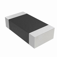
NTHS0603N10N1502JE Vishay, NTHS0603N10N1502JE Datasheet - Page 44

NTHS0603N10N1502JE
Manufacturer Part Number
NTHS0603N10N1502JE
Description
THERMISTOR NTC 15K OHM 5% 0603
Manufacturer
Vishay
Series
NTHSr
Specifications of NTHS0603N10N1502JE
Resistance In Ohms @ 25°c
15K
Resistance Tolerance
±5%
B Value Tolerance
±3%
B25/75
3500K
Mounting Type
Surface Mount
Package / Case
0603 (1608 Metric)
Lead Free Status / RoHS Status
Lead free by exemption / RoHS Compliant
B0/50
-
B25/50
-
B25/85
-
B25/100
-
Operating Temperature
-
Power - Max
-
Lead Length
-
Lead Free Status / Rohs Status
Lead free / RoHS Compliant
Other names
541-1114-2
Available stocks
Company
Part Number
Manufacturer
Quantity
Price
Part Number:
NTHS0603N10N1502JE
Manufacturer:
VISHAY/威世
Quantity:
20 000
44
10.4.4
Accelerated Program
The abort condition is indicated by DQ1 = 1, DQ7 = DATA# (for the last address location loaded), DQ6 =
toggle, and DQ5= 0. A Write-to-Buffer-Abort Reset command sequence must be written to reset the device
for the next operation.
Note that the Secured Silicon Sector, autoselect, and CFI functions are unavailable when a program
operation is in progress. This flash device is capable of handling multiple write buffer programming operations
on the same write buffer address range without intervening erases. For applications requiring incremental bit
programming, a modified programming method is required; please contact your local Spansion
representative. Any bit in a write buffer address range cannot be programmed from 0 back to a 1.
Attempting to do so may cause the device to set DQ5=1, of cause the DQ7 and DQ6 status bits to indicate
the operation was successful. However, a succeeding read shows that the data is still 0. Only erase
operations can convert a 0 to a 1.
The device offers accelerated program operations through the WP#/ACC or ACC pin depending on the
particular product. When the system asserts V
voltage on the WP#/ACC or ACC pin to accelerate the operation. Note that the WP#/ACC pin must not be at
V
internal pull-up; when unconnected, WP# is at V
Figure 10.1 on page 45
Operations–AC Characteristics on page 64
HH
Write an Address/Data pair to a different write-buffer-page than the one selected by the Starting Address
during the write buffer data loading stage of the operation.
Write data other than the Confirm Command after the specified number of data load cycles.
for operations other than accelerated programming, or device damage may result. WP# contains an
illustrates the algorithm for the program operation. Refer to the Erase and Program
S29GL-N MirrorBit
for parameters, and
D a t a
HH
®
IH
Flash Family
on the WP#/ACC or ACC pin. The device uses the higher
.
S h e e t
Figure 15.3 on page 65
S29GL-N_01_12 October 29, 2008
for timing diagrams.


