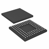
ADUC7121BBCZ-RL Analog Devices Inc, ADUC7121BBCZ-RL Datasheet - Page 78

ADUC7121BBCZ-RL
Manufacturer Part Number
ADUC7121BBCZ-RL
Description
PRECISION ANALOG MCU I.C
Manufacturer
Analog Devices Inc
Series
MicroConverter® ADuC7xxxr
Datasheet
1.ADUC7121BBCZ.pdf
(96 pages)
Specifications of ADUC7121BBCZ-RL
Core Processor
ARM7
Core Size
16/32-Bit
Speed
41.78MHz
Connectivity
I²C, SPI, UART/USART
Peripherals
POR, PWM, WDT
Number Of I /o
32
Program Memory Size
126KB (63K x 16)
Program Memory Type
FLASH
Ram Size
8K x 8
Voltage - Supply (vcc/vdd)
3 V ~ 3.6 V
Data Converters
A/D 9x12b, D/A 4x12b
Oscillator Type
Internal
Operating Temperature
-10°C ~ 95°C
Package / Case
108-LFBGA, CSPBGA
Lead Free Status / RoHS Status
Lead free / RoHS Compliant
Eeprom Size
-
Lead Free Status / RoHS Status
Lead free / RoHS Compliant
Other names
ADUC7121BBCZ-RL
ADUC7121BBCZ-RLTR
ADUC7121BBCZ-RLTR
Available stocks
Company
Part Number
Manufacturer
Quantity
Price
Company:
Part Number:
ADUC7121BBCZ-RL
Manufacturer:
Analog Devices Inc
Quantity:
10 000
ADuC7121
PLACLK Register
PLACLK is the clock selection for the flip-flops of Block 0 and
Block 1. The maximum frequency when using the GPIO pins as
the clock input for the PLA blocks is 41.78 MHz.
Name:
Address:
Default value:
Access:
Table 103. PLACLK MMR Bit Descriptions
Bit
7
6:4
3
2:0
PLAIRQ Register
PLAIRQ enables IRQ0 and/or IRQ1 and selects the source
of the normal interrupt request IRQ (IRQ).
Name:
Address:
Default value:
Access:
Table 104. PLAIRQ MMR Bit Descriptions
Bit
15:13
12
Value
000
001
010
011
100
101
Other
000
001
010
011
100
101
Other
Value
Description
Reserved.
Block 1 clock source selection.
GPIO clock on P0.5 of the P0.5/ CS /PLAI[10]/
ADC
GPIO clock on P0.0 of the P0.0/SCL0/PLAI[5] pin.
GPIO clock on the P0.7 of the P0.7/TRST/PLAI[3] pin.
HCLK (core clock).
OCLK (32.768 kHz external crystal).
Timer1 overflow.
Reserved.
Reserved.
Block 0 clock source selection.
GPIO clock on P0.5. on P0.5 of the P0.5/ CS /
PLAI[10]/ADC
GPIO clock on P0.0 of the P0.0/SCL0/PLAI[5] pin.
GPIO clock on P0.7 of the P0.7/TRST/PLAI[3] pin.
HCLK (core clock).
OCLK (32.768 kHz external crystal).
Timer1 overflow.
Reserved.
PLACLK
0xFFFF0B40
0x00
Read and write
PLAIRQ
0xFFFF0B44
0x0000
Read and write
CONVST
Description
Reserved.
PLA IRQ1 enable bit.
Set by the user to enable IRQ1 output from
the PLA.
Cleared by the user to disable IRQ1 output
from the PLA.
pin.
CONVST
pin.
Rev. 0 | Page 78 of 96
Bit
11:8
7:5
4
3:0
PLAADC Register
PLAADC is the PLA source for the ADC start conversion signal.
Name:
Address:
Default value:
Access:
Table 105. PLAADC MMR Bit Descriptions
Bit
31:5
4
3:0
PLADIN Register
PLADIN is a data input MMR for PLA.
Name:
Address:
Default value:
Access:
Table 106. PLADIN MMR Bit Descriptions
Bit
31:16
15:0
Value
0000
0001
1111
Value
0000
0001
1111
0000
0001
1111
Description
Reserved.
Input bit from Element 15 to Element 0.
PLAADC
0xFFFF0B48
0x00000000
Read and write
PLADIN
0xFFFF0B4C
0x00000000
Read and write
Description
Reserved.
ADC start conversion enable bit.
Set by the user to enable an ADC start
conversion from the PLA.
Cleared by the user to disable an ADC start
conversion from the PLA.
ADC start conversion source.
PLA Element 0.
PLA Element 1.
PLA Element 15.
Description
PLA IRQ1 source.
PLA Element 0.
PLA Element 1.
PLA Element 15.
Reserved.
PLA IRQ0 enable bit.
Set by the user to enable IRQ0 output from
the PLA.
Cleared by the user to disable IRQ0 output
from the PLA.
PLA IRQ0 source.
PLA Element 0.
PLA Element 1.
PLA Element 15.


