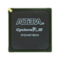
EP3C5E144A7N Altera, EP3C5E144A7N Datasheet - Page 182

EP3C5E144A7N
Manufacturer Part Number
EP3C5E144A7N
Description
Cyclone III
Manufacturer
Altera
Datasheet
1.EP3C5E144A7N.pdf
(274 pages)
Specifications of EP3C5E144A7N
Family Name
Cyclone III
Number Of Logic Blocks/elements
5136
# I/os (max)
94
Frequency (max)
437.5MHz
Process Technology
65nm
Operating Supply Voltage (typ)
1.2V
Logic Cells
5136
Ram Bits
423936
Operating Supply Voltage (min)
1.15V
Operating Supply Voltage (max)
1.25V
Operating Temp Range
-40C to 125C
Operating Temperature Classification
Automotive
Mounting
Surface Mount
Pin Count
144
Package Type
EQFP
Lead Free Status / Rohs Status
Compliant
Available stocks
Company
Part Number
Manufacturer
Quantity
Price
- Current page: 182 of 274
- Download datasheet (6Mb)
9–22
Figure 9–7. In-System Programming of Serial Configuration Devices
Notes to
(1) Connect these pull-up resistors to the V
(2) The nCEO pin is left unconnected or used as a user I/O pin when it does not feed the nCE pin of another device.
(3) Power up the V
(4) The MSEL pin settings vary for different configuration voltage standards and POR time. To connect MSEL[3..0], refer to
(5) These are dual-purpose I/O pins. This nCSO pin functions as the FLASH_NCE pin in AP mode. The ASDO pin functions as the DATA[1] pin in
(6) The diodes and capacitors must be placed as close as possible to the Cyclone III device family. Ensure that the diodes and capacitors maintain a
(7) When cascading Cyclone III device family in a multi-device AS configuration, connect the repeater buffers between the master and slave devices
Cyclone III Device Handbook, Volume 1
page
other AP and FPP modes.
maximum AC voltage of 4.1 V. The external diodes and capacitors are required to prevent damage to the Cyclone III device family AS configuration
input pins due to possible overshoot when programming the serial configuration device using a download cable. For effective voltage clamping,
Altera recommends using the Schottky diode, which has a relatively lower forward diode voltage (VF) than the switching and Zener diodes. For
more information about the interface guidelines using Schottky diodes, refer to
Devices.
for DATA[0] and DCLK. All I/O inputs must maintain a maximum AC voltage of 4.1 V. The output resistance of the repeater buffers must fit the
maximum overshoot equation outlined in
Figure
9–11. Connect the MSEL pins directly to V
9–7:
CC
of the ByteBlaster II or USB-Blaster download cable with the 3.3-V supply.
Configuration Device
Figure 9–7
Serial
Chapter 9: Configuration, Design Security, and Remote System Upgrades in the Cyclone III Device Family
DCLK
DATA
ASDI
nCS
10
shows the download cable connections to the serial configuration device.
CCIO
V CCIO (1)
kΩ
“Configuration and JTAG Pin I/O Requirements” on page 9–7.
supply of the bank in which the pin resides.
10
kΩ
CCA
GND
10
or ground.
V CCIO (1)
(6)
kΩ
10 pf
(6)
3.3 V
GND
GND
3.3 V
10
10 pf
V CCIO (1)
kΩ
10 pf
GND
3.3 V
3.3 V
GND
10 pf
AN 523: Cyclone III Configuration Interface Guidelines with EPCS
ByteBlaster II or USB Blaster
nSTATUS
CONF_DONE
nCONFIG
nCE
DATA[0] (7)
DCLK (7)
nCSO (5)
ASDO (5)
Pin 1
10-Pin Male Header
Cyclone III Device Family
3.3 V (3)
GND
GND
MSEL[3..0]
© December 2009 Altera Corporation
nCEO
N.C. (2)
(4)
Configuration Features
Table 9–7 on
Related parts for EP3C5E144A7N
Image
Part Number
Description
Manufacturer
Datasheet
Request
R

Part Number:
Description:
Cyclone III Device Data Sheet
Manufacturer:
ALTERA [Altera Corporation]
Datasheet:

Part Number:
Description:
CYCLONE II STARTER KIT EP2C20N
Manufacturer:
Altera
Datasheet:

Part Number:
Description:
CPLD, EP610 Family, ECMOS Process, 300 Gates, 16 Macro Cells, 16 Reg., 16 User I/Os, 5V Supply, 35 Speed Grade, 24DIP
Manufacturer:
Altera Corporation
Datasheet:

Part Number:
Description:
CPLD, EP610 Family, ECMOS Process, 300 Gates, 16 Macro Cells, 16 Reg., 16 User I/Os, 5V Supply, 15 Speed Grade, 24DIP
Manufacturer:
Altera Corporation
Datasheet:

Part Number:
Description:
Manufacturer:
Altera Corporation
Datasheet:

Part Number:
Description:
CPLD, EP610 Family, ECMOS Process, 300 Gates, 16 Macro Cells, 16 Reg., 16 User I/Os, 5V Supply, 30 Speed Grade, 24DIP
Manufacturer:
Altera Corporation
Datasheet:

Part Number:
Description:
High-performance, low-power erasable programmable logic devices with 8 macrocells, 10ns
Manufacturer:
Altera Corporation
Datasheet:

Part Number:
Description:
High-performance, low-power erasable programmable logic devices with 8 macrocells, 7ns
Manufacturer:
Altera Corporation
Datasheet:

Part Number:
Description:
Classic EPLD
Manufacturer:
Altera Corporation
Datasheet:

Part Number:
Description:
High-performance, low-power erasable programmable logic devices with 8 macrocells, 10ns
Manufacturer:
Altera Corporation
Datasheet:

Part Number:
Description:
Manufacturer:
Altera Corporation
Datasheet:

Part Number:
Description:
Manufacturer:
Altera Corporation
Datasheet:

Part Number:
Description:
Manufacturer:
Altera Corporation
Datasheet:


