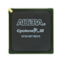
EP3C5E144A7N Altera, EP3C5E144A7N Datasheet - Page 202

EP3C5E144A7N
Manufacturer Part Number
EP3C5E144A7N
Description
Cyclone III
Manufacturer
Altera
Datasheet
1.EP3C5E144A7N.pdf
(274 pages)
Specifications of EP3C5E144A7N
Family Name
Cyclone III
Number Of Logic Blocks/elements
5136
# I/os (max)
94
Frequency (max)
437.5MHz
Process Technology
65nm
Operating Supply Voltage (typ)
1.2V
Logic Cells
5136
Ram Bits
423936
Operating Supply Voltage (min)
1.15V
Operating Supply Voltage (max)
1.25V
Operating Temp Range
-40C to 125C
Operating Temperature Classification
Automotive
Mounting
Surface Mount
Pin Count
144
Package Type
EQFP
Lead Free Status / Rohs Status
Compliant
Available stocks
Company
Part Number
Manufacturer
Quantity
Price
- Current page: 202 of 274
- Download datasheet (6Mb)
9–42
Cyclone III Device Handbook, Volume 1
Figure 9–19
MasterBlaster, USB-Blaster, ByteBlaster II, or ByteBlasterMV cable.
Figure 9–19. Multi-Device PS Configuration Using a USB-Blaster, MasterBlaster, ByteBlaster II,
ByteBlasterMV, or Ethernet Blaster Cable
Notes to
(1) The pull-up resistor must be connected to the same supply voltage as the V
(2) You only need the pull-up resistors on DATA[0] and DCLK if the download cable is the only configuration scheme
(3) Pin 6 of the header is a V
(4) Connect the pull-up resistor to the V
(5) The nCEO pin of the last device in the chain is left unconnected or used as a user I/O pin.
(6) The MSEL pin settings vary for different configuration voltage standards and POR time. To connect MSEL[3..0]
(7) Power up the V
10
used on your board. This is to ensure that DATA[0] and DCLK are not left floating after configuration. For example,
if you are also using a configuration device, you do not need the pull-up resistors on DATA[0] and DCLK.
device. For this value, refer to the
this pin is a no connect. In USB-Blaster, ByteBlaster II, and Ethernet Blaster, this pin is connected to nCE when it is
used for AS programming. Otherwise, it is a no connect.
for PS configuration schemes, refer to
Third-party programmers must switch to 2.5 V. Pin 4 of the header is a V
The MasterBlaster cable can receive power from either 5.0- or 3.3-V circuit boards, DC power supply, or 5.0 V from
the USB cable. For this value, refer to the
kΩ
V
CCA
Figure
10
Chapter 9: Configuration, Design Security, and Remote System Upgrades in the Cyclone III Device Family
(2)
kΩ
V CCA (1)
(1)
shows PS configuration for multi Cyclone III device family using a
9–19:
V CCIO (4)
CC
of the ByteBlaster II, USB-Blaster, or ByteBlasterMV cable with a 2.5- V supply from V
10
GND
kΩ
IO
Cyclone III Device Family 2
Cyclone III Device Family 1
reference voltage for the MasterBlaster output driver. V
nCONFIG
DATA[0]
MSEL[3..0] (6)
nCE
nCE
MSEL[3..0]
(6)
nCONFIG
DATA[0]
MasterBlaster Serial/USB Communications Cable User
CCIO
CONF_DONE
CONF_DONE
Table 9–7 on page
nSTATUS
supply voltage of the I/O bank in which the nCE pin resides.
nSTATUS
MasterBlaster Serial/USB Communications Cable User
DCLK
DCLK
nCEO
nCEO
10
N.C. (5)
kΩ
V CCA (1)
9–11. Connect the MSEL pins directly to V
V CCA (1)
10
10
(2)
kΩ
kΩ
V CCA (1)
CC
power supply for the MasterBlaster cable.
CCA
© December 2009 Altera Corporation
supply.
IO
must match the V
10-Pin Male Header
(Passive Serial Mode)
Pin 1
Guide. In ByteBlasterMV,
Download Cable
Configuration Features
GND
Guide.
V CCA (7)
CCA
CCA
VIO (3)
GND
CCA
or GND.
of the
.
Related parts for EP3C5E144A7N
Image
Part Number
Description
Manufacturer
Datasheet
Request
R

Part Number:
Description:
Cyclone III Device Data Sheet
Manufacturer:
ALTERA [Altera Corporation]
Datasheet:

Part Number:
Description:
CYCLONE II STARTER KIT EP2C20N
Manufacturer:
Altera
Datasheet:

Part Number:
Description:
CPLD, EP610 Family, ECMOS Process, 300 Gates, 16 Macro Cells, 16 Reg., 16 User I/Os, 5V Supply, 35 Speed Grade, 24DIP
Manufacturer:
Altera Corporation
Datasheet:

Part Number:
Description:
CPLD, EP610 Family, ECMOS Process, 300 Gates, 16 Macro Cells, 16 Reg., 16 User I/Os, 5V Supply, 15 Speed Grade, 24DIP
Manufacturer:
Altera Corporation
Datasheet:

Part Number:
Description:
Manufacturer:
Altera Corporation
Datasheet:

Part Number:
Description:
CPLD, EP610 Family, ECMOS Process, 300 Gates, 16 Macro Cells, 16 Reg., 16 User I/Os, 5V Supply, 30 Speed Grade, 24DIP
Manufacturer:
Altera Corporation
Datasheet:

Part Number:
Description:
High-performance, low-power erasable programmable logic devices with 8 macrocells, 10ns
Manufacturer:
Altera Corporation
Datasheet:

Part Number:
Description:
High-performance, low-power erasable programmable logic devices with 8 macrocells, 7ns
Manufacturer:
Altera Corporation
Datasheet:

Part Number:
Description:
Classic EPLD
Manufacturer:
Altera Corporation
Datasheet:

Part Number:
Description:
High-performance, low-power erasable programmable logic devices with 8 macrocells, 10ns
Manufacturer:
Altera Corporation
Datasheet:

Part Number:
Description:
Manufacturer:
Altera Corporation
Datasheet:

Part Number:
Description:
Manufacturer:
Altera Corporation
Datasheet:

Part Number:
Description:
Manufacturer:
Altera Corporation
Datasheet:


