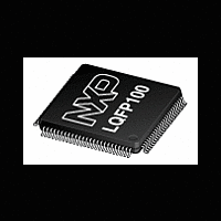
LPC2364HBD100 NXP Semiconductors, LPC2364HBD100 Datasheet - Page 15

LPC2364HBD100
Manufacturer Part Number
LPC2364HBD100
Description
LPC2364HBD100/LQFP100/TRAYBDP/
Manufacturer
NXP Semiconductors
Series
LPC2300r
Datasheet
1.LPC2364FBD100551.pdf
(59 pages)
Specifications of LPC2364HBD100
Core Processor
ARM7
Core Size
16/32-Bit
Speed
72MHz
Connectivity
CAN, Ethernet, I²C, Microwire, SPI, SSI, SSP, UART/USART, USB
Peripherals
Brown-out Detect/Reset, DMA, I²S, POR, PWM, WDT
Number Of I /o
70
Program Memory Size
128KB (128K x 8)
Program Memory Type
FLASH
Ram Size
34K x 8
Voltage - Supply (vcc/vdd)
3 V ~ 3.6 V
Data Converters
A/D 6x10b; D/A 1x10b
Oscillator Type
Internal
Operating Temperature
-40°C ~ 125°C
Package / Case
100-LQFP
Processor Series
LPC23
Core
ARM7TDMI-S
3rd Party Development Tools
MDK-ARM, RL-ARM, ULINK2, SAB-TFBGA100
Lead Free Status / RoHS Status
Lead free / RoHS Compliant
Eeprom Size
-
Lead Free Status / Rohs Status
Details
Available stocks
Company
Part Number
Manufacturer
Quantity
Price
Company:
Part Number:
LPC2364HBD100
Manufacturer:
NXP
Quantity:
479
Company:
Part Number:
LPC2364HBD100
Manufacturer:
NXP Semiconductors
Quantity:
10 000
Part Number:
LPC2364HBD100
Manufacturer:
NXP/恩智浦
Quantity:
20 000
Company:
Part Number:
LPC2364HBD100,551
Manufacturer:
NXP Semiconductors
Quantity:
10 000
Part Number:
LPC2364HBD100,551
Manufacturer:
NXP/恩智浦
Quantity:
20 000
NXP Semiconductors
Table 4.
[1]
[2]
[3]
[4]
[5]
[6]
[7]
LPC2364_65_66_67_68_6
Product data sheet
Symbol
TCK
RTCK
RSTOUT
RESET
XTAL1
XTAL2
RTCX1
RTCX2
V
V
V
V
V
VREF
VBAT
SS
SSA
DD(3V3)
DD(DCDC)(3V3)
DDA
5 V tolerant pad providing digital I/O functions with TTL levels and hysteresis.
5 V tolerant pad providing digital I/O functions (with TTL levels and hysteresis) and analog input. When configured as a DAC input,
digital section of the pad is disabled.
5 V tolerant pad providing digital I/O with TTL levels and hysteresis and analog output function. When configured as the DAC output,
digital section of the pad is disabled.
Open-drain 5 V tolerant digital I/O pad, compatible with I
output functionality. When power is switched off, this pin connected to the I
Open-drain configuration applies to all functions on this pin.
Pad provides digital I/O and USB functions (LPC2364/66/68 only). It is designed in accordance with the USB specification, revision 2.0
(Full-speed and Low-speed mode only).
5 V tolerant pad with 5 ns glitch filter providing digital I/O functions with TTL levels and hysteresis.
5 V tolerant pad with 20 ns glitch filter providing digital I/O function with TTL levels and hysteresis.
Pin description
Pin
5
100
14
17
22
23
16
18
15, 31,
41, 55,
72, 97,
83
11
28, 54,
71,
96
13, 42,
84
10
12
19
[1]
[11]
[7]
[8][9]
[8][9]
[8]
[8]
[10]
[12]
[13]
[14]
[14]
[14]
[1]
…continued
Ball
C1
B2
-
F3
H2
G3
F2
G1
B3, B7,
C9, F1,
G7, J6,
K3
E1
A3, C10,
H9,
K2
A7, E4,
H6
E2
E3
G2
[7]
[8]
[1]
[11]
[12]
[14]
[14]
[1]
[8][9]
[13]
[8][9]
[8]
[14]
[10]
Type
I
I/O
O
I
I
O
I
O
I
I
I
I
I
I
I
Description
TCK — Test Clock for JTAG interface. This clock must be slower than
the CPU clock (CCLK) for the JTAG interface to operate
RTCK — JTAG interface control signal.
Note: LOW on this pin while RESET is LOW enables ETM pins (P2[9:0]) to
operate as trace port after reset.
RSTOUT — This is a 3.3 V pin. LOW on this pin indicates
LPC2364/65/66/67/68 being in Reset state.
Note: This pin is available in LPC2364FBD100, LPC2365FBD100,
LPC2366FBD100, LPC2367FBD100, and LPC2368FBD100 devices only
(LQFP100 package).
External reset input: A LOW on this pin resets the device, causing I/O
ports and peripherals to take on their default states, and processor
execution to begin at address 0. TTL with hysteresis, 5 V tolerant.
Input to the oscillator circuit and internal clock generator circuits.
Output from the oscillator amplifier.
Input to the RTC oscillator circuit.
Output from the RTC oscillator circuit.
ground: 0 V reference.
analog ground: 0 V reference. This should nominally be the same voltage
as V
3.3 V supply voltage: This is the power supply voltage for the I/O ports.
3.3 V DC-to-DC converter supply voltage: This is the supply voltage for
the on-chip DC-to-DC converter only.
analog 3.3 V pad supply voltage: This should be nominally the same
voltage as V
voltage is used to power the ADC and DAC.
ADC reference: This should be nominally the same voltage as V
should be isolated to minimize noise and error. Level on this pin is used as
a reference for ADC and DAC.
RTC pin power supply: 3.3 V on this pin supplies the power to the RTC
peripheral.
Rev. 06 — 1 February 2010
SS
2
C-bus 400 kHz specification. This pad requires an external pull-up to provide
, but should be isolated to minimize noise and error.
DD(3V3)
but should be isolated to minimize noise and error. This
2
C-bus is floating and does not disturb the I
LPC2364/65/66/67/68
Single-chip 16-bit/32-bit microcontrollers
© NXP B.V. 2010. All rights reserved.
2
C lines.
DD(3V3)
15 of 59
1
⁄
6
but
of


