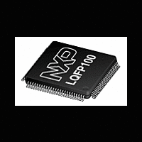
LPC2364HBD100 NXP Semiconductors, LPC2364HBD100 Datasheet - Page 21

LPC2364HBD100
Manufacturer Part Number
LPC2364HBD100
Description
LPC2364HBD100/LQFP100/TRAYBDP/
Manufacturer
NXP Semiconductors
Series
LPC2300r
Datasheet
1.LPC2364FBD100551.pdf
(59 pages)
Specifications of LPC2364HBD100
Core Processor
ARM7
Core Size
16/32-Bit
Speed
72MHz
Connectivity
CAN, Ethernet, I²C, Microwire, SPI, SSI, SSP, UART/USART, USB
Peripherals
Brown-out Detect/Reset, DMA, I²S, POR, PWM, WDT
Number Of I /o
70
Program Memory Size
128KB (128K x 8)
Program Memory Type
FLASH
Ram Size
34K x 8
Voltage - Supply (vcc/vdd)
3 V ~ 3.6 V
Data Converters
A/D 6x10b; D/A 1x10b
Oscillator Type
Internal
Operating Temperature
-40°C ~ 125°C
Package / Case
100-LQFP
Processor Series
LPC23
Core
ARM7TDMI-S
3rd Party Development Tools
MDK-ARM, RL-ARM, ULINK2, SAB-TFBGA100
Lead Free Status / RoHS Status
Lead free / RoHS Compliant
Eeprom Size
-
Lead Free Status / Rohs Status
Details
Available stocks
Company
Part Number
Manufacturer
Quantity
Price
Company:
Part Number:
LPC2364HBD100
Manufacturer:
NXP
Quantity:
479
Company:
Part Number:
LPC2364HBD100
Manufacturer:
NXP Semiconductors
Quantity:
10 000
Part Number:
LPC2364HBD100
Manufacturer:
NXP/恩智浦
Quantity:
20 000
Company:
Part Number:
LPC2364HBD100,551
Manufacturer:
NXP Semiconductors
Quantity:
10 000
Part Number:
LPC2364HBD100,551
Manufacturer:
NXP/恩智浦
Quantity:
20 000
NXP Semiconductors
LPC2364_65_66_67_68_6
Product data sheet
7.8.1 Features
7.9.1 Features
7.9 Ethernet
Additionally, any pin on Port 0 and Port 2 (total of 42 pins) providing a digital function can
be programmed to generate an interrupt on a rising edge, a falling edge, or both. The
edge detection is asynchronous, so it may operate when clocks are not present such as
during Power-down mode. Each enabled interrupt can be used to wake up the chip from
Power-down mode.
The Ethernet block contains a full featured 10 Mbit/s or 100 Mbit/s Ethernet MAC
designed to provide optimized performance through the use of DMA hardware
acceleration. Features include a generous suite of control registers, half or full duplex
operation, flow control, control frames, hardware acceleration for transmit retry, receive
packet filtering and wake-up on LAN activity. Automatic frame transmission and reception
with scatter-gather DMA off-loads many operations from the CPU.
The Ethernet block and the CPU share a dedicated AHB subsystem that is used to access
the Ethernet SRAM for Ethernet data, control, and status information. All other AHB traffic
in the LPC2364/65/66/67/68 takes place on a different AHB subsystem, effectively
separating Ethernet activity from the rest of the system. The Ethernet DMA can also
access the USB SRAM if it is not being used by the USB block.
The Ethernet block interfaces between an off-chip Ethernet PHY using the Reduced MII
(RMII) protocol and the on-chip Media Independent Interface Management (MIIM) serial
bus.
•
•
•
•
•
•
•
Bit level set and clear registers allow a single instruction to set or clear any number of
bits in one port.
Direction control of individual bits.
All I/O default to inputs after reset.
Backward compatibility with other earlier devices is maintained with legacy Port 0 and
Port 1 registers appearing at the original addresses on the APB.
Ethernet standards support:
– Supports 10 Mbit/s or 100 Mbit/s PHY devices including 10 Base-T, 100 Base-TX,
– Fully compliant with IEEE standard 802.3.
– Fully compliant with 802.3x full duplex flow control and half duplex back pressure.
– Flexible transmit and receive frame options.
– Virtual Local Area Network (VLAN) frame support.
Memory management:
– Independent transmit and receive buffers memory mapped to shared SRAM.
– DMA managers with scatter/gather DMA and arrays of frame descriptors.
– Memory traffic optimized by buffering and pre-fetching.
Enhanced Ethernet features:
100 Base-FX, and 100 Base-T4.
Rev. 06 — 1 February 2010
LPC2364/65/66/67/68
Single-chip 16-bit/32-bit microcontrollers
© NXP B.V. 2010. All rights reserved.
21 of 59


