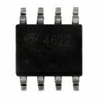
AO4622 Alpha & Omega Semiconductor Inc, AO4622 Datasheet

AO4622
Specifications of AO4622
Available stocks
Related parts for AO4622
AO4622 Summary of contents
Page 1
... AO4622 Complementary Enhancement Mode Field Effect Transistor General Description The AO4622/L uses advanced trench technology MOSFETs to provide excellent R and low gate charge. The DS(ON) complementary MOSFETs may be used to form a level shifted high side switch, and for a host of other applications.AO4622 and AO4622L are electrically identical. ...
Page 2
... AO4622 N-Channel Electrical Characteristics (T Symbol Parameter STATIC PARAMETERS BV Drain-Source Breakdown Voltage DSS I Zero Gate Voltage Drain Current DSS I Gate-Body leakage current GSS V Gate Threshold Voltage GS(th state drain current D(ON) R Static Drain-Source On-Resistance DS(ON) g Forward Transconductance FS V Diode Forward Voltage SD I Maximum Body-Diode Continuous Current ...
Page 3
... AO4622 N-CHANNEL TYPICAL ELECTRICAL AND THERMAL CHARACTERISTICS 60 6V 10V (Volts) DS Figure 1: On-Region Characteristics 100 =2. (A) D Figure 3: On-Resistance vs. Drain Current and Gate Voltage (Volts) GS Figure 5: On-Resistance vs. Gate-Source Voltage Alpha & Omega Semiconductor, Ltd 1.60 1.40 1.20 1.00 V =4.5V GS 0.80 V =10V GS 20 ...
Page 4
... AO4622 N-Channel TYPICAL ELECTRICAL AND THERMAL CHARACTERISTICS =10V DS I =7. (nC) g Figure 7: Gate-Charge Characteristics 100.0 1ms 10.0 10ms R 1s 1.0 DS(ON) limited 10s 0.1 T =150°C J(Max) T =25°C A 0.0 0 (Volts) DS Figure 9: Maximum Forward Biased Safe Operating Area (Note θJA R =62.5° ...
Page 5
... AO4622 + VDC - Vgs Isd Alpha & Omega Semiconductor, Ltd. Gate Charge Test Circuit & Waveform Vgs 10V + Vds VDC - DUT R e sistive S w itch ircu it & iod very T est C ircuit & W ave Isd + Qgs Qgd Charge ff Idt dI/ www.aosmd.com ...
Page 6
... AO4622 P-Channel Electrical Characteristics (T Symbol Parameter STATIC PARAMETERS BV Drain-Source Breakdown Voltage DSS I Zero Gate Voltage Drain Current DSS I Gate-Body leakage current GSS V Gate Threshold Voltage GS(th state drain current D(ON) R Static Drain-Source On-Resistance DS(ON) g Forward Transconductance FS V Diode Forward Voltage SD Maximum Body-Diode Continuous Current ...
Page 7
... AO4622 TYPICAL ELECTRICAL AND THERMAL CHARACTERISTICS: P-CHANNEL 25 -10V -3.5V 20 -4.5V - (Volts) DS Fig 1: On-Region Characteristics =-2. (A) D Figure 3: On-Resistance vs. Drain Current and Gate Voltage (Volts) GS Figure 5: On-Resistance vs. Gate-Source Voltage Alpha & Omega Semiconductor, Ltd =-2. 0.5 1.6 1.4 1 =-4.5V 0.8 GS 0.6 - 1.0E+02 I =-5A 1.0E+ ...
Page 8
... AO4622 TYPICAL ELECTRICAL AND THERMAL CHARACTERISTICS: P-CHANNEL =-10V (nC) g Figure 7: Gate-Charge Characteristics 100 10 1ms R 1 DS(ON) limited 10s 0 T =150°C J(Max) T =25° 0 (Volts) DS Figure 9: Maximum Forward Biased Safe Operating Area (Note θJA J, =62.5°C/W θJA 1 0.1 Single Pulse ...
Page 9
... AO4622 - VDC + Vgs Ig Vds Vgs Vds + Isd Alpha & Omega Semiconductor, Ltd. Gate Charge Test Circuit & Waveform Vgs -10V - Vds VDC + DUT R esistive S witching Test C ircuit & W aveform s RL Vgs - DU T Vdd VDC + iod e R ecovery Test C ircuit & W aveform s ...


