FDC3601N Fairchild Semiconductor, FDC3601N Datasheet
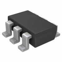
MOSFET N-CH DUAL 100V SSOT-6

FDC3601N

Manufacturer Part Number
FDC3601N
Description
MOSFET N-CH DUAL 100V SSOT-6
Manufacturer
Fairchild Semiconductor
Series
PowerTrench®r
Datasheet

Specifications of FDC3601N

Fet Type
2 N-Channel (Dual)
Fet Feature
Logic Level Gate
Rds On (max) @ Id, Vgs
500 mOhm @ 1A, 10V
Drain To Source Voltage (vdss)
100V
Current - Continuous Drain (id) @ 25° C
1A
Vgs(th) (max) @ Id
4V @ 250µA
Gate Charge (qg) @ Vgs
5nC @ 10V
Input Capacitance (ciss) @ Vds
153pF @ 50V
Power - Max
700W
Mounting Type
Surface Mount
Package / Case
6-SSOT, SuperSOT-6
Configuration
Dual
Transistor Polarity
N-Channel
Resistance Drain-source Rds (on)
0.5 Ohm @ 10 V
Forward Transconductance Gfs (max / Min)
3.6 S
Drain-source Breakdown Voltage
100 V
Gate-source Breakdown Voltage
+/- 20 V
Continuous Drain Current
1 A
Power Dissipation
960 mW
Maximum Operating Temperature
+ 150 C
Mounting Style
SMD/SMT
Minimum Operating Temperature
- 55 C
Module Configuration
Dual
Continuous Drain Current Id
1A
Drain Source Voltage Vds
100V
On Resistance Rds(on)
500mohm
Rds(on) Test Voltage Vgs
10V
Rohs Compliant
Yes
Threshold Voltage Vgs Typ
2.6V
Lead Free Status / RoHS Status
Lead free / RoHS Compliant

Available stocks

Company
Part Number
Manufacturer
Quantity
Price
Part Number:
FDC3601N
Manufacturer:
FSC
Quantity:
15 600
Part Number:
FDC3601N
Manufacturer:
Fairchild Semiconductor
Quantity:
59 148
Part Number:
FDC3601N
Manufacturer:
FAIRCHILD
Quantity:
8 000
Part Number:
FDC3601N
0
Company:
Part Number:
FDC3601N
Quantity:
12 996
FDC3601N
Dual N-Channel 100V Specified PowerTrench MOSFET
General Description
These N-Channel 100V specified MOSFETs are
produced using Fairchild Semiconductor's advanced
PowerTrench process that has been especially tailored
to minimize on-state resistance and yet maintain low
gate charge for superior switching performance.
These devices have been designed to offer exceptional
power dissipation in a very small footprint for
applications where the bigger more expensive SO-8
and TSSOP-8 packages are impractical.
Applications
• Load switch
• Battery protection
• Power management
2001 Fairchild Semiconductor Corporation
Absolute Maximum Ratings
Symbol
V
V
I
P
T
Thermal Characteristics
R
R
Package Marking and Ordering Information
D
J
DSS
GSS
D
, T
JA
JC
Device Marking
STG
SuperSOT
.601
Drain-Source Voltage
Gate-Source Voltage
Drain Current
Power Dissipation for Single Operation
Operating and Storage Junction Temperature Range
Thermal Resistance, Junction-to-Ambient
Thermal Resistance, Junction-to-Case
D1
S1
TM
-6
D2
– Continuous
– Pulsed
FDC3601N
Device
G1
Parameter
S2
G2
T
A
=25
o
C unless otherwise noted
Reel Size
7’’
(Note 1a)
(Note 1a)
(Note 1b)
(Note 1a)
(Note 1c)
(Note 1)
Features
1.0 A, 100 V.
Low gate charge (3.7nC typical)
Fast switching speed.
High performance trench technology for extremely
SuperSOT
low R
(smaller than standard SO-8); low profile (1mm thick).
DS(ON)
TM
.
4
5
6
-6 package: small footprint 72%
Tape width
R
R
DS(ON)
DS(ON)
8mm
Ratings
55 to +150
0.96
100
130
1.0
4.0
0.9
0.7
60
= 500 m @ V
= 550 m @ V
20
3
2
1
August 2001
GS
GS
FDC3601N Rev C(W)
= 10 V
= 6.0 V
3000 units
Quantity
Units
C/W
C/W
W
V
V
A
C

Related parts for FDC3601N

FDC3601N Summary of contents

Page 1

... C unless otherwise noted A (Note 1a) (Note 1a) (Note 1b) (Note 1c) (Note 1a) (Note 1) Reel Size 7’’ August 2001 R = 500 DS(ON 550 6.0 V DS(ON package: small footprint 72 Ratings Units 100 1.0 A 4.0 0.96 W 0.9 0 +150 C 130 C/W 60 C/W Tape width Quantity 8mm 3000 units FDC3601N Rev C(W) ...

Page 2

... Min Typ Max Units 100 V 105 mV 100 nA –100 –5 mV/ C 370 500 m 396 550 685 976 3 A 3.6 S 153 3 0 0.8 A 0.8 1 180°C/W when mounted on a minimum pad. FDC3601N Rev C(W) ...

Page 3

... Figure 6. Body Diode Forward Voltage Variation with Source Current and Temperature 4.0V GS 4.5V 5.0V 6.0V 10V DRAIN CURRENT ( 0. 125 GATE TO SOURCE VOLTAGE (V) GS Gate-to-Source Voltage 125 -55 C 0.2 0.4 0.6 0 BODY DIODE FORWARD VOLTAGE (V) SD FDC3601N Rev C( 1.2 ...

Page 4

... Figure 10. Single Pulse Maximum 0.01 0 TIME (sec 1MHz C ISS DRAIN TO SOURCE VOLTAGE (V) DS SINGLE PULSE R = 180°C 25° 100 1000 t , TIME (sec) 1 Power Dissipation. R ( 180°C Duty Cycle 100 FDC3601N Rev C(W) 50 1000 ...

Page 5

... TRADEMARKS The following are registered and unregistered trademarks Fairchild Semiconductor owns or is authorized to use and is not intended exhaustive list of all such trademarks. ACEx™ FAST Bottomless™ FASTr™ CoolFET™ FRFET™ CROSSVOLT™ GlobalOptoisolator™ GTO™ DenseTrench™ ...

Related keywords