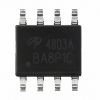
AO4803A Alpha & Omega Semiconductor Inc, AO4803A Datasheet
Home Discrete Semiconductor Products MOSFETs - Arrays AO4803A
Manufacturer Part Number
AO4803A
Description
MOSFET DUAL P-CH -30V -5A 8-SOIC
Manufacturer
Alpha & Omega Semiconductor Inc
Specifications of AO4803A
Fet Type
2 P-Channel (Dual)
Fet Feature
Logic Level Gate
Rds On (max) @ Id, Vgs
46 mOhm @ 5A, 10V
Drain To Source Voltage (vdss)
30V
Current - Continuous Drain (id) @ 25° C
5A
Vgs(th) (max) @ Id
2.5V @ 250µA
Gate Charge (qg) @ Vgs
16nC @ 10V
Input Capacitance (ciss) @ Vds
830pF @ 15V
Power - Max
2W
Mounting Type
Surface Mount
Package / Case
8-SOIC
Lead Free Status / RoHS Status
Lead free / RoHS Compliant
Available stocks
Rev 1: Dec 2009
Absolute Maximum Ratings T
Parameter
Drain-Source Voltage
Gate-Source Voltage
Continuous Drain
Current
Pulsed Drain Current
Avalanche Current
Avalanche energy L=0.1mH
Power Dissipation
Junction and Storage Temperature Range
Thermal Characteristics
Maximum Junction-to-Ambient
Maximum Junction-to-Ambient
Maximum Junction-to-Lead
The AO4803A uses advanced trench technology to
provide excellent R
device is suitable for use as a load switch or in PWM
applications.
General Description
Top View
B
Parameter
C
DS(ON)
Pin1
SOIC-8
C
T
T
T
T
A
A
A
A
=25°C
=70°C
=25°C
=70°C
with low gate charge. This
C
Bottom View
A
A D
A
=25°C unless otherwise noted
t ≤ 10s
Steady-State
Steady-State
Symbol
V
V
I
I
I
E
P
T
Symbol
D
DM
AS
www.aosmd.com
DS
GS
AS
D
J
, T
, I
R
R
, E
AR
STG
θJA
θJL
AR
S2
G2
S1
G1
Top View
1
2
3
4
Product Summary
V
I
R
R
100% UIS Tested
100% R
D
DS
DS(ON)
DS(ON)
(at V
8
7
6
5
Typ
48
74
35
(at V
(at V
GS
g
=-10V)
Tested
30V
D2
D2
D1
D1
GS
GS
Maximum
-55 to 150
=-10V)
= -4.5V)
±20
-30
-30
1.3
17
14
-5
-4
2
G1
Dual P-Channel MOSFET
Max
62.5
110
40
D1
S1
AO4803A
G2
-30V
-5A
< 46mΩ
< 74mΩ
Units
Units
°C/W
°C/W
°C/W
mJ
°C
Page 1 of 6
W
D2
S2
V
V
A
A
Related parts for AO4803A
AO4803A Summary of contents
... General Description The AO4803A uses advanced trench technology to provide excellent R with low gate charge. This DS(ON) device is suitable for use as a load switch or in PWM applications. SOIC-8 Top View Bottom View Pin1 Absolute Maximum Ratings T =25°C unless otherwise noted A Parameter ...
... Ratings are based on low frequency and duty cycles to keep J(MAX) and lead to ambient. θJL =150°C. The SOA curve provides a single pulse rating. J(MAX) www.aosmd.com AO4803A Min Typ Max Units - =55°C ...
... Figure 2: Transfer Characteristics (Note E) 1.8 1.6 1.4 1 Figure 4: On-Resistance vs. Junction Temperature 1.0E+02 I =-5A D 1.0E+01 40 1.0E+00 1.0E-01 1.0E-02 1.0E-03 1.0E-04 1.0E-05 0 Figure 6: Body-Diode Characteristics (Note E) www.aosmd.com AO4803A 125°C 25°C 1.5 2 2.5 3 3.5 4 4.5 5 5.5 -V (Volts =-10V =-4. =- ...
... A 10.0 R DS(ON) limited T =125°C A 1.0 0.1 T J(Max) T =25°C A 0.0 0.01 100 1000 (µs) A Figure 10: Maximum Forward Biased Safe 0.1 Pulse Width (s) www.aosmd.com AO4803A C iss C oss (Volts) DS 10µs 100µs 1ms 10ms DC =150°C 10s 0 100 -V (Volts) ...
... Single Pulse 0.001 0.00001 0.0001 0.001 Figure 12: Normalized Maximum Transient Thermal Impedance (Note F) Rev 1: Dec 2009 In descending order D=0.5, 0.3, 0.1, 0.05, 0.02, 0.01, single pulse P D 0.01 0.1 1 Pulse Width (s) 40 www.aosmd.com AO4803A 100 1000 Page ...
... DUT Resistive Switching Test Circuit & Waveforms Vgs d(on Vdd VDC + Vds 1 Vds - Vgs Vdd VDC Id + Vgs Diode Recovery Test Circuit & Waveforms Idt Vgs -Isd - Vdd VDC - -Vds www.aosmd.com AO4803A Qg Qgd Charge t off t t d(off) f 90% 10% BV DSS dI/ Vdd Page ...
Related keywords
ao4805 ao4803a ao4800b ao4800 AO4803A datasheet AO4803A data sheet AO4803A pdf datasheet AO4803A component AO4803A part AO4803A distributor AO4803A RoHS AO4803A datasheet download


