FDG6302P Fairchild Semiconductor, FDG6302P Datasheet
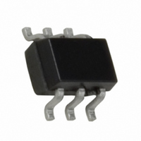
MOSFET P-CH DUAL 25V SC70-6

FDG6302P

Manufacturer Part Number
FDG6302P
Description
MOSFET P-CH DUAL 25V SC70-6
Manufacturer
Fairchild Semiconductor
Datasheet

Specifications of FDG6302P

Fet Type
2 P-Channel (Dual)
Fet Feature
Logic Level Gate
Rds On (max) @ Id, Vgs
10 Ohm @ 140mA, 4.5V
Drain To Source Voltage (vdss)
25V
Current - Continuous Drain (id) @ 25° C
140mA
Vgs(th) (max) @ Id
1.5V @ 250µA
Gate Charge (qg) @ Vgs
0.31nC @ 4.5V
Input Capacitance (ciss) @ Vds
12pF @ 10V
Power - Max
300mW
Mounting Type
Surface Mount
Package / Case
SC-70-6, SC-88, SOT-363
Lead Free Status / RoHS Status
Lead free / RoHS Compliant

Available stocks

Company
Part Number
Manufacturer
Quantity
Price
Part Number:
FDG6302P-NL
Manufacturer:
AD
Quantity:
1 345
Symbol
V
V
I
P
T
ESD
THERMAL CHARACTERISTICS
R
.
Absolute Maximum Ratings
D
FDG6302P
Dual P-Channel, Digital FET
J
*
DSS
GSS
D
General Description
These dual P-Channel logic level enhancement mode
field effect transistors are produced using Fairchild's
proprietary, high cell density, DMOS technology. This
very high density process is especially tailored to
minimize on-state resistance. This device has been
designed especially for low voltage applications as a
replacement for bipolar digital transistors and small
signal MOSFETs.
,T
JA
Units inside the carrier can be of either orientation and will not affect the functionality of the device.
The pinouts are symmetrical; pin 1 and 4 are interchangeable.
STG
SC70-6
Parameter
Drain-Source Voltage
Gate-Source Voltage
Drain/Output Current
Maximum Power Dissipation
Operating and Storage Temperature Range
Electrostatic Discharge Rating MIL-STD-883D
Human Body Model (100 pF / 1500 )
Thermal Resistance, Junction-to-Ambient
SC70-6
D1
SOT-23
G2
- Continuous
- Pulsed
S2
S1
T
A
= 25°C unless otherwise noted
SuperSOT
G1
D2
(Note 1)
(Note 1)
TM
-6
Features
SuperSOT
-25 V, -0.14 A continuous, -0.4 A peak.
Very low level gate drive requirements allowing direct
operation in 3 V circuits (V
Gate-Source Zener for ESD ruggedness
(>6kV Human Body Model).
Compact industry standard SC70-6 surface
mount package.
TM
-8
R
R
DS(ON)
DS(ON)
FDG6302P
1 or 4
2 or 5
-55 to 150
3 or 6
= 10
= 13
-0.14
-0.4
415
6.0
-25
0.3
-8
*
SO-8
@ V
@ V
GS(th)
GS
GS
< 1.5 V).
= -4.5 V,
= -2.7 V.
SOT-223
4 or 1
6 or 3
5 or 2
July 1999
FDG6302P Rev.F1
*
°C/W
Units
°C
kV
W
V
V
A

Related parts for FDG6302P

FDG6302P Summary of contents

Page 1

... Human Body Model). Compact industry standard SC70-6 surface mount package. TM SuperSOT -6 SuperSOT 25°C unless otherwise noted A (Note 1) (Note 1) July 1999 -4.5 V, DS(ON -2.7 V. DS(ON) GS < 1.5 V). GS(th) SO SOT-223 * FDG6302P -25 -8 -0.14 -0.4 0.3 -55 to 150 6.0 415 * Units °C kV °C/W FDG6302P Rev.F1 ...

Page 2

... GS GEN -0. -4 -0.25 A (Note 415 O C/W on minimum pad mounting on FR-4 board in still air. JA Min Typ Max - - 55°C -10 J -100 -0.65 -0 =125° 10.4 13 -0. 0.22 0.31 0.12 0.05 -0.25 -0.8 -1.2 is guaranteed JC FDG6302P Rev.F1 Units µA µ ...

Page 3

... Drain Current and Gate Voltage -0.07A 125° 25° 2.5 3 3 GATE TO SOURCE VOLTAGE (V) GS Gate-to-Source Voltage 125°C A 25°C -55°C 0.2 0.4 0.6 0 BODY DIODE FORWARD VOLTAGE (V) SD Variation with Source Current and Temperature. -4.5V 0.2 5 1.2 FDG6302P Rev.F ...

Page 4

... Thermal characterization performed using the conditions described in note 1. C iss C oss C rss MHz 0.2 0 DRAIN TO SOURCE VOLTAGE (V) DS SINGLE PULSE R =415°C 25°C A 0.001 0.01 0 SINGLE PULSE TIME (SEC) Dissipation. R ( =415 °C/W JA P(pk ( Duty Cycle 100 20 200 200 FDG6302P Rev.F ...

Page 5

... TRADEMARKS The following are registered and unregistered trademarks Fairchild Semiconductor owns or is authorized to use and is not intended exhaustive list of all such trademarks. ACEx™ Bottomless™ CoolFET™ CROSSVOLT™ CMOS FACT™ FACT Quiet Series™ FAST FASTr™ GTO™ ...

Related keywords