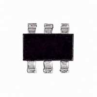
FDC638APZ Fairchild Semiconductor, FDC638APZ Datasheet - Page 4

FDC638APZ
Manufacturer Part Number
FDC638APZ
Description
MOSFET P-CH 20V 4.5A SSOT-6
Manufacturer
Fairchild Semiconductor
Series
PowerTrench®r
Datasheet
1.FDC638APZ.pdf
(5 pages)
Specifications of FDC638APZ
Fet Type
MOSFET P-Channel, Metal Oxide
Fet Feature
Logic Level Gate
Rds On (max) @ Id, Vgs
43 mOhm @ 4.5A, 4.5V
Drain To Source Voltage (vdss)
20V
Current - Continuous Drain (id) @ 25° C
4.5A
Vgs(th) (max) @ Id
1.5V @ 250µA
Gate Charge (qg) @ Vgs
12nC @ 4.5V
Input Capacitance (ciss) @ Vds
1000pF @ 10V
Power - Max
800mW
Mounting Type
Surface Mount
Package / Case
6-SSOT, SuperSOT-6
Configuration
Single Quad Drain
Transistor Polarity
P-Channel
Resistance Drain-source Rds (on)
0.043 Ohm @ 4.5 V
Forward Transconductance Gfs (max / Min)
18 S
Drain-source Breakdown Voltage
20 V
Gate-source Breakdown Voltage
+/- 12 V
Continuous Drain Current
4.5 A
Power Dissipation
1600 mW
Maximum Operating Temperature
+ 150 C
Mounting Style
SMD/SMT
Minimum Operating Temperature
- 55 C
Lead Free Status / RoHS Status
Lead free / RoHS Compliant
Other names
FDC638APZTR
Available stocks
Company
Part Number
Manufacturer
Quantity
Price
Company:
Part Number:
FDC638APZ
Manufacturer:
Fairchild Semiconductor
Quantity:
33 090
Part Number:
FDC638APZ
Manufacturer:
FAIRCHILD/仙童
Quantity:
20 000
Part Number:
FDC638APZ-NL
Manufacturer:
FAIRCHILD/仙童
Quantity:
20 000
FDC638APZ Rev.B
Typical Characteristics
Figure 11. Single Pulse Maximum Power Di
Figure 9.
1E-3
1E-4
1E-5
0.01
0.1
Figure 7.
50
40
30
20
10
0
5
4
3
2
1
0
1
10
0
0
-3
V
I
GS
D
T
= -4.5A
Gate Leakage Current vs Gate to
= 0V
J
-V
= 150
2
GS
10
Gate Charge Characteristics
-2
, GATE TO SOURCE VOLTAGE(V)
Source Voltage
o
5
C
Q
g
t, PULSE WIDTH (s)
, GATE CHARGE(nC)
4
10
V
SINGLE PULSE
DD
-1
= -5V
10
6
T
J
10
= 25°C unless otherwise noted
V
T
0
DD
J
8
= 25
SINGLE PULSE
R
T
= -15V
A
V
θ
15
JA
o
=25
DD
C
10
= 156
= -10V
o
10
C
1
ssipation
o
C/W
10
20
12
2
4
Figure 12. Transient Thermal Response Curve
0.001
2000
1000
0.01
0.01
100
100
0.1
0.1
10
70
0.1
1
1
10
0.1
-4
Figure 8.
DUTY CYCLE-DESCENDING ORDER
D = 0.5
SINGLE PULSE
r
Figure 10.
f = 1MHz
V
DS(on)
GS
0.2
0.1
0.05
0.02
0.01
t, RECTANGULAR PULSE DURATION (s)
-V
-V DS , DRAIN to SOURCE VOLTAGE (V)
10
= 0V
LIMIT
DS
-3
to Source Voltage
, DRAIN TO SOURCE VOLTAGE (V)
Operating Area
Capacitance vs Drain
NOTES:
DUTY FACTOR: D = t
PEAK T
10
Forward Bias Safe
-2
1
1
SINGLE PULSE
T J = MAX RATED
T A = 25
J
= P
10
DM
-1
O
C
x Z
P
θJA
DM
1
10
/t
x R
C
2
C
C
0
rss
oss
iss
θJA
10
t
1
www.fairchildsemi.com
+ T
t
2
10
A
10
1
100ms
10us
100us
1ms
10ms
1s
DC
20
50
10
2


