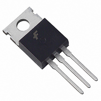
MTP3055VL Fairchild Semiconductor, MTP3055VL Datasheet - Page 2

MTP3055VL
Manufacturer Part Number
MTP3055VL
Description
MOSFET N-CH 60V 12A TO-220
Manufacturer
Fairchild Semiconductor
Datasheet
1.MTP3055VL.pdf
(3 pages)
Specifications of MTP3055VL
Fet Type
MOSFET N-Channel, Metal Oxide
Fet Feature
Logic Level Gate
Rds On (max) @ Id, Vgs
180 mOhm @ 6A, 5V
Drain To Source Voltage (vdss)
60V
Current - Continuous Drain (id) @ 25° C
12A
Vgs(th) (max) @ Id
2V @ 250µA
Gate Charge (qg) @ Vgs
10nC @ 5V
Input Capacitance (ciss) @ Vds
570pF @ 25V
Power - Max
48W
Mounting Type
Through Hole
Package / Case
TO-220-3 (Straight Leads)
Configuration
Single
Transistor Polarity
N-Channel
Resistance Drain-source Rds (on)
0.18 Ohm @ 5 V
Drain-source Breakdown Voltage
60 V
Gate-source Breakdown Voltage
+/- 15 V
Continuous Drain Current
12 A
Power Dissipation
48000 mW
Maximum Operating Temperature
+ 175 C
Mounting Style
Through Hole
Minimum Operating Temperature
- 65 C
Lead Free Status / RoHS Status
Lead free / RoHS Compliant
Other names
MTP3055VLFS
Available stocks
Company
Part Number
Manufacturer
Quantity
Price
Company:
Part Number:
MTP3055VL
Manufacturer:
FUJI
Quantity:
6 000
Part Number:
MTP3055VL
Manufacturer:
FAIRCHILD/仙童
Quantity:
20 000
Electrical Characteristics
Off Characteristics
On Characteristics
Dynamic Characteristics
Switching Characteristics
Drain-Source Diode Characteristics and Maximum Ratings
1. R
2. Pulse Test: Pulse Width 300 s, Duty Cycle 2.0%
DRAIN-SOURCE AVALANCHE RATINGS
Notes:
w
I
BV
I
I
I
V
R
V
g
C
C
C
t
t
t
t
Q
Q
Q
I
I
V
t
Symbol
AR
DSS
GSSF
GSSR
d(on)
r
d(off)
f
S
SM
rr
FS
BV
V
DSS
GS(th)
DS(on)
DS(on)
iss
oss
rss
SD
g
gs
gd
JA
DSS
GS(th)
T
T
DSS
J
J
is the sum of the juntion-to-case and case-to-ambient thermal resistance.
Single Pulse Drain-Source
Avalanche Energy
Maximum Drain-Source Avalanche Current
Drain-Source Breakdown
Voltage
Breakdown Voltage Temperature
Coefficient
Zero Gate Voltage Drain Current
Gate-Body Leakage Current,
Forward
Gate-Body Leakage Current,
Reverse
Gate Threshold Voltage
Gate Threshold Voltage
Temperature Coefficient
Static Drain-Source
On-Resistance
Drain-Source On-Voltage
On-Resistance
Forward Transconductance
Input Capacitance
Output Capacitance
Reverse Transfer Capacitance
Turn-On Delay Time
Turn-On Rise Time
Turn-Off Delay Time
Turn-Off Fall Time
Total Gate Charge
Gate-Source Charge
Gate-Drain Charge
Maximum Continuous Drain-Source Diode Forward Current
Maximum Pulsed Drain-Source Diode Forward Current
Drain-Source Diode Forward
Voltage
Drain-Source Reverse Recovery
Time
Parameter
(Note 2)
(Note 2)
T
C
= 25°C unless otherwise noted
V
V
I
V
V
150 C
V
V
V
I
V
V
V
V
f = 1.0 MHz
V
V
V
I
V
I
D
D
D
F
DD
GS
DS
DS
GS
GS
DS
GS
GS
DS
DS
DD
GS
DS
GS
=12 A, di/dt = 100A/ s
= 250 A, Referenced to 25 C
= 250 A, Referenced to 25 C
= 12 A, V
= 25 V, I
= 0 V, I
= 60 V, V
= 60 V, V
= 15 V, V
= -15 V, V
= V
= 5 V,I
= 5 V,I
= 8 V, I
= 25 V, V
= 30 V, I
= 5 V, R
= 48 V,
= 0 V, I
(Note 2)
Test Conditions
GS
, I
D
D
D
D
D
S
GS
= 6 A,
= 12 A
GEN
D
D
= 6 A
= 12 A
= 250 A
= 250 A
GS
DS
GS
GS
DS
= 12 A
= 12 A,
= 5 V
= 0 V, T
= 0 V
= 0 V,
= 9.1
= 0 V
= 0 V
J
(Note 2)
(Note 2)
(Note 2)
=
Min
60
1
5
0.100
Typ
345
110
1.6
8.7
7.8
1.7
3.2
55
30
55
-4
0.180
Max
-100
100
100
570
160
190
2.6
1.3
72
12
10
40
20
30
90
10
12
42
2
MTP3055VL Rev. A1
Units
mV/ C
mV/ C
mJ
nC
nC
nC
nA
nA
pF
pF
pF
nS
ns
ns
ns
ns
A
V
V
V
S
A
A
V
A


