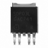
SPD50P03L G Infineon Technologies, SPD50P03L G Datasheet - Page 6

SPD50P03L G
Manufacturer Part Number
SPD50P03L G
Description
MOSFET P-CH 30V 50A TO-252
Manufacturer
Infineon Technologies
Series
OptiMOS™r
Datasheet
1.SPD50P03L_G.pdf
(9 pages)
Specifications of SPD50P03L G
Package / Case
DPak, TO-252 (4 leads + tab)
Fet Type
MOSFET P-Channel, Metal Oxide
Fet Feature
Logic Level Gate
Rds On (max) @ Id, Vgs
7 mOhm @ 50A, 10V
Drain To Source Voltage (vdss)
30V
Current - Continuous Drain (id) @ 25° C
50A
Vgs(th) (max) @ Id
2V @ 250µA
Gate Charge (qg) @ Vgs
126nC @ 10V
Input Capacitance (ciss) @ Vds
6880pF @ 25V
Power - Max
150W
Mounting Type
Surface Mount
Minimum Operating Temperature
- 55 C
Configuration
Single Dual Source
Transistor Polarity
P-Channel
Resistance Drain-source Rds (on)
0.007 Ohm @ 10 V
Drain-source Breakdown Voltage
30 V
Gate-source Breakdown Voltage
+/- 20 V
Continuous Drain Current
50 A
Power Dissipation
150000 mW
Maximum Operating Temperature
+ 175 C
Mounting Style
SMD/SMT
Fall Time
104 ns
Rise Time
21.7 ns
Package
DPAK 5pin (TO-252 5pin)
Vds (max)
-30.0 V
Rds (on) (max) (@10v)
7.0 mOhm
Rds (on) (max) (@4.5v)
125.0 mOhm
Rds (on) (max) (@2.5v)
-
Lead Free Status / RoHS Status
Lead free / RoHS Compliant
Lead Free Status / RoHS Status
Lead free / RoHS Compliant, Lead free / RoHS Compliant
Other names
SP000086729
SP000371908
SPD50P03L G
SPD50P03LGINTR
SPD50P03LGXT
SP000371908
SPD50P03L G
SPD50P03LGINTR
SPD50P03LGXT
Rev. 1.8
9 Drain-source on-state resistance
R
11 Typ. capacitances
C =f(V
DS(on)
10
10
10
11
4
3
2
DS
=f(T
9
7
5
3
10000
1000
100
0
-60
); V
j
); I
GS
D
=0 V; f =1 MHz
-20
=-50 A; V
5
20
98 %
10
GS
-V
T
=-10 V
DS
j
60
Crss
[°C]
Ciss
[V]
Coss
15
typ.
100
20
140
180
page 6
25
10 Typ. gate threshold voltage
V
12 Forward characteristics of reverse diode
I
parameter: T
F
GS(th)
=f(V
1000
100
2.5
1.5
0.5
10
=f(T
SD
2
1
0
1
-60
)
0
j
); V
j
GS
-20
0.5
=V
DS
20
; I
D
1
=-250 µA
-V
T
98%.
j
SD
60
[°C]
typ.
2%
[V]
1.5
175 °C, typ
25 °C, typ
25 °C, 98%
175 °C, 98%
100
SPD50P03L
SPD50P03L G
2
140
2008-07-10
180
2.5


