IPB034N03L G Infineon Technologies, IPB034N03L G Datasheet - Page 3
IPB034N03L G
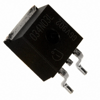
Manufacturer Part Number
IPB034N03L G
Description
MOSFET N-CH 30V 80A TO-263-3
Manufacturer
Infineon Technologies
Series
OptiMOS™r
Datasheet
1.IPP034N03L_G.pdf
(10 pages)
Specifications of IPB034N03L G
Package / Case
D²Pak, TO-263 (2 leads + tab)
Fet Type
MOSFET N-Channel, Metal Oxide
Fet Feature
Logic Level Gate
Rds On (max) @ Id, Vgs
3.4 mOhm @ 30A, 10V
Drain To Source Voltage (vdss)
30V
Current - Continuous Drain (id) @ 25° C
80A
Vgs(th) (max) @ Id
2.2V @ 250µA
Gate Charge (qg) @ Vgs
51nC @ 10V
Input Capacitance (ciss) @ Vds
5300pF @ 15V
Power - Max
94W
Mounting Type
Surface Mount
Minimum Operating Temperature
- 55 C
Configuration
Single
Transistor Polarity
N-Channel
Resistance Drain-source Rds (on)
0.0034 Ohm @ 10 V
Drain-source Breakdown Voltage
30 V
Gate-source Breakdown Voltage
+/- 20 V
Continuous Drain Current
80 A
Power Dissipation
94000 mW
Maximum Operating Temperature
+ 175 C
Mounting Style
SMD/SMT
Drain Source Voltage Vds
30V
On Resistance Rds(on)
2.8mohm
Rds(on) Test Voltage Vgs
10V
Operating Temperature Range
-55°C To +175°C
Transistor Case Style
TO-263
Rohs Compliant
Yes
Lead Free Status / RoHS Status
Lead free / RoHS Compliant
Lead Free Status / RoHS Status
Lead free / RoHS Compliant, Lead free / RoHS Compliant
Other names
IPB034N03LGINTR
IPB034N03LGXT
SP000304126
IPB034N03LGXT
SP000304126


Rev. 2.0
6)
Parameter
Dynamic characteristics
Input capacitance
Output capacitance
Reverse transfer capacitance
Turn-on delay time
Rise time
Turn-off delay time
Fall time
Gate Charge Characteristics
Gate to source charge
Gate charge at threshold
Gate to drain charge
Switching charge
Gate charge total
Gate plateau voltage
Gate charge total
Gate charge total, sync. FET
Output charge
Reverse Diode
Diode continuous forward current
Diode pulse current
Diode forward voltage
Reverse recovery charge
See figure 16 for gate charge parameter definition
5)
Symbol Conditions
C
C
C
t
t
t
t
Q
Q
Q
Q
Q
V
Q
Q
Q
I
I
V
Q
d(on)
r
d(off)
f
S
S,pulse
rss
plateau
SD
iss
oss
gs
g(th)
gd
sw
g
g
g(sync)
oss
rr
V
f =1 MHz
V
I
V
V
V
V
V
V
V
T
V
T
V
di
D
page 3
C
j
GS
DD
DD
GS
DD
GS
DS
GS
DD
GS
R
=30 A, R
=25 ° C
F
=25 °C
=15 V, I
/dt =400 A/µs
=0 V, V
=15 V, V
=15 V, I
=0 to 4.5 V
=15 V, I
=0 to 10 V
=0.1 V,
=0 to 4.5 V
=15 V, V
=0 V, I
F
F
G
DS
=30 A,
=I
D
D
=1.6 W
GS
GS
=30 A,
=30 A,
=15 V,
S
=10 V,
=0 V
,
min.
-
-
-
-
-
-
-
-
-
-
-
-
-
-
-
-
-
-
-
-
Values
4000
1400
0.83
typ.
9.2
6.4
5.4
6.3
5.6
2.9
81
35
12
11
25
51
21
37
-
-
-
IPB034N03L G
IPP034N03L G
max.
5300
1900
320
1.1
80
20
-
-
-
-
-
-
-
-
-
-
-
-
-
-
Unit
pF
ns
nC
V
nC
A
V
nC
2010-02-19
Related parts for IPB034N03L G
Image
Part Number
Description
Manufacturer
Datasheet
Request
R

Part Number:
Description:
Manufacturer:
Infineon Technologies AG
Datasheet:
Part Number:
Description:
Manufacturer:
Infineon Technologies AG
Datasheet:
Part Number:
Description:
Manufacturer:
Infineon Technologies AG
Datasheet:
Part Number:
Description:
Manufacturer:
Infineon Technologies AG
Datasheet:
Part Number:
Description:
Manufacturer:
Infineon Technologies AG
Datasheet:
Part Number:
Description:
Manufacturer:
Infineon Technologies AG
Datasheet:
Part Number:
Description:
Manufacturer:
Infineon Technologies AG
Datasheet:
Part Number:
Description:
16-bit microcontroller with 2x2 KByte RAM
Manufacturer:
Infineon Technologies AG
Datasheet:
Part Number:
Description:
NPN silicon RF transistor
Manufacturer:
Infineon Technologies AG
Datasheet:
Part Number:
Description:
NPN silicon RF transistor
Manufacturer:
Infineon Technologies AG
Datasheet:
Part Number:
Description:
NPN silicon RF transistor
Manufacturer:
Infineon Technologies AG
Datasheet:
Part Number:
Description:
NPN silicon RF transistor
Manufacturer:
Infineon Technologies AG
Datasheet:
Part Number:
Description:
Si-MMIC-amplifier in SIEGET 25-technologie
Manufacturer:
Infineon Technologies AG
Datasheet:
Part Number:
Description:
IGBT Power Module
Manufacturer:
Infineon Technologies AG
Datasheet:
Part Number:
Description:
IC for switching-mode power supplies
Manufacturer:
Infineon Technologies AG
Datasheet: