FDB045AN08A0 Fairchild Semiconductor, FDB045AN08A0 Datasheet - Page 4
FDB045AN08A0
Manufacturer Part Number
FDB045AN08A0
Description
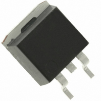
MOSFET N-CH 75V 90A D2PAK
Manufacturer
Fairchild Semiconductor
Series
PowerTrench®r
Datasheet
1.FDB045AN08A0.pdf
(11 pages)
Specifications of FDB045AN08A0
Fet Type
MOSFET N-Channel, Metal Oxide
Fet Feature
Standard
Rds On (max) @ Id, Vgs
4.5 mOhm @ 80A, 10V
Drain To Source Voltage (vdss)
75V
Current - Continuous Drain (id) @ 25° C
90A
Vgs(th) (max) @ Id
4V @ 250µA
Gate Charge (qg) @ Vgs
138nC @ 10V
Input Capacitance (ciss) @ Vds
6600pF @ 25V
Power - Max
310W
Mounting Type
Surface Mount
Package / Case
D²Pak, TO-263 (2 leads + tab)
Configuration
Single
Transistor Polarity
N-Channel
Resistance Drain-source Rds (on)
0.0045 Ohm @ 10 V
Drain-source Breakdown Voltage
75 V
Gate-source Breakdown Voltage
+/- 20 V
Continuous Drain Current
80 A
Power Dissipation
310000 mW
Maximum Operating Temperature
+ 175 C
Mounting Style
SMD/SMT
Minimum Operating Temperature
- 55 C
Lead Free Status / RoHS Status
Lead free / RoHS Compliant
Other names
FDB045AN08A0TR
Available stocks
Company
Part Number
Manufacturer
Quantity
Price
Company:

Part Number:
FDB045AN08A0
Manufacturer:
FSC
Quantity:
4 300


FDB045AN08A0 Rev. A1
Typical Characteristics
Figure 9.
1000
2000
Figure 5.
100
150
120
0.1
10
7
6
5
4
3
90
60
30
1
0
0.1
4.0
0
Figure 7.
T
T
SINGLE PULSE
OPERATION IN THIS
PULSE DURATION = 80μs
DUTY CYCLE = 0.5% MAX
V
J
C
PULSE DURATION = 80μs
DUTY CYCLE = 0.5% MAX
LIMITED BY r
DD
T
= MAX RATED
= 25
Drain to Source On Resistance vs Drain
J
= 15V
AREA MAY BE
= 25
o
Forward Bias Safe Operating Area
C
V
o
V
C
DS
GS
4.5
20
, DRAIN TO SOURCE VOLTAGE (V)
, GATE TO SOURCE VOLTAGE (V)
DS(ON)
Transfer Characteristics
T
V
V
I
J
D
1
GS
GS
, DRAIN CURRENT (A)
= 175
Current
= 10V
= 6V
o
C
5.0
40
T
C
10
= 25°C unless otherwise noted
T
J
DC
= -55
5.5
60
10μs
10ms
100μs
1ms
o
C
100
6.0
80
NOTE: Refer to Fairchild Application Notes AN7514 and AN7515
500
100
150
120
10
Figure 10.
Figure 6.
90
60
30
1
2.5
2.0
1.5
1.0
0.5
0
.01
-80
0
Resistance vs Junction Temperature
Figure 8. Saturation Characteristics
If R = 0
t
If R ≠ 0
t
AV
AV
STARTING T
PULSE DURATION = 80μs
DUTY CYCLE = 0.5% MAX
= (L)(I
= (L/R)ln[(I
-40
V
GS
Unclamped Inductive Switching
AS
V
Normalized Drain to Source On
= 10V
DS
)/(1.3*RATED BV
T
0.1
J
J
t
, DRAIN TO SOURCE VOLTAGE (V)
AS
, JUNCTION TEMPERATURE (
AV
= 150
0
*R)/(1.3*RATED BV
, TIME IN AVALANCHE (ms)
0.5
Capability
o
C
40
DSS
1
V
GS
PULSE DURATION = 80μs
DUTY CYCLE = 0.5% MAX
- V
80
= 6V
DD
DSS
STARTING T
)
1.0
V
- V
GS
120
DD
10
= 10V, I
o
V
) +1]
V
C)
GS
GS
J
www.fairchildsemi.com
= 7V
T
= 5V
160
= 25
C
D
= 25
=80A
o
C
o
C
100
200
1.5
Related parts for FDB045AN08A0
Image
Part Number
Description
Manufacturer
Datasheet
Request
R

Part Number:
Description:
Fairchild Semiconductor [IGBT MODULE]
Manufacturer:
Fairchild Semiconductor
Datasheet:

Part Number:
Description:
Discrete Semiconductor Modules
Manufacturer:
Fairchild Semiconductor
Part Number:
Description:
Discrete Semiconductor Modules
Manufacturer:
Fairchild Semiconductor
Part Number:
Description:
This N-Channel MOSFET is produced using Fairchild Semiconductor’s advanced Power Trench® process
Manufacturer:
Fairchild Semiconductor
Datasheet:
Part Number:
Description:
This N-Channel MOSFET is produced using Fairchild Semiconductor’s advanced Power Trench® process
Manufacturer:
Fairchild Semiconductor
Datasheet:
Part Number:
Description:
This N-Channel MOSFET is produced using Fairchild Semiconductor’s advanced PowerTrench® process
Manufacturer:
Fairchild Semiconductor
Datasheet:
Part Number:
Description:
This N-Channel MOSFET is produced using Fairchild Semiconductor’s advanced PowerTrench® process
Manufacturer:
Fairchild Semiconductor
Datasheet:
Part Number:
Description:
This N-Channel MOSFET is produced using Fairchild Semiconductor’s advanced Power Trench® process
Manufacturer:
Fairchild Semiconductor
Datasheet:
Part Number:
Description:
This N-Channel logic Level MOSFETs are produced using Fairchild Semiconductor‘s advanced Power Trench® process that has been special tailored to minimize the on-state resistance and yet maintain superior switching performance
Manufacturer:
Fairchild Semiconductor
Datasheet:
Part Number:
Description:
This N-Channel MOSFET is produced using Fairchild Semiconductor’s advanced Power Trench® process
Manufacturer:
Fairchild Semiconductor
Datasheet:
Part Number:
Description:
This N-Channel SyncFET™ is produced using Fairchild Semiconductor’s advanced PowerTrench® process
Manufacturer:
Fairchild Semiconductor
Datasheet:
Part Number:
Description:
This N-Channel SyncFET™ is produced using Fairchild Semiconductor’s advanced PowerTrench® process
Manufacturer:
Fairchild Semiconductor
Datasheet:
Part Number:
Description:
This N-Channel SyncFET™ is produced using Fairchild Semiconductor’s advanced PowerTrench® process
Manufacturer:
Fairchild Semiconductor
Datasheet:
Part Number:
Description:
This N-Channel logic Level MOSFETs are produced using Fairchild Semiconductor‘s advanced Power Trench® process that has been special tailored to minimize the on-state resistance and yet maintain superior switching performance
Manufacturer:
Fairchild Semiconductor
Datasheet:
Part Number:
Description:
This N-Channel MOSFET is produced using Fairchild Semiconductor’s advanced Power Trench® process that has been especially tailored to minimize the on-state resistance and yet maintain superior switching performance
Manufacturer:
Fairchild Semiconductor
Datasheet: