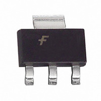
NDT014 Fairchild Semiconductor, NDT014 Datasheet - Page 3

NDT014
Manufacturer Part Number
NDT014
Description
MOSFET N-CH 60V 2.7A SOT-223-4
Manufacturer
Fairchild Semiconductor
Datasheet
1.NDT014.pdf
(7 pages)
Specifications of NDT014
Fet Type
MOSFET N-Channel, Metal Oxide
Fet Feature
Standard
Rds On (max) @ Id, Vgs
200 mOhm @ 1.6A, 10V
Drain To Source Voltage (vdss)
60V
Current - Continuous Drain (id) @ 25° C
2.7A
Vgs(th) (max) @ Id
4V @ 250µA
Gate Charge (qg) @ Vgs
11nC @ 10V
Input Capacitance (ciss) @ Vds
155pF @ 25V
Power - Max
1.1W
Mounting Type
Surface Mount
Package / Case
SOT-223 (3 leads + Tab), SC-73, TO-261
Configuration
Single Dual Drain
Transistor Polarity
N-Channel
Resistance Drain-source Rds (on)
0.2 Ohms
Forward Transconductance Gfs (max / Min)
2 S
Drain-source Breakdown Voltage
60 V
Gate-source Breakdown Voltage
+/- 20 V
Continuous Drain Current
+/- 2.7 A
Power Dissipation
3 W
Maximum Operating Temperature
+ 150 C
Mounting Style
SMD/SMT
Minimum Operating Temperature
- 65 C
Continuous Drain Current Id
2.7A
Drain Source Voltage Vds
60V
On Resistance Rds(on)
180mohm
Rds(on) Test Voltage Vgs
10V
Threshold Voltage Vgs Typ
3V
Rohs Compliant
Yes
Fall Time
10 ns
Rise Time
64 ns
Lead Free Status / RoHS Status
Lead free / RoHS Compliant
Other names
NDT014TR
Available stocks
Company
Part Number
Manufacturer
Quantity
Price
Part Number:
NDT014
Manufacturer:
FAIRCHILD/仙童
Quantity:
20 000
Company:
Part Number:
NDT014L
Manufacturer:
FSC
Quantity:
10 000
Company:
Part Number:
NDT014L
Manufacturer:
FSC
Quantity:
2 656
Part Number:
NDT014L
Manufacturer:
FAIRCHILD/仙童
Quantity:
20 000
Electrical Characteristics
Symbol
DRAIN-SOURCE DIODE CHARACTERISTICS AND MAXIMUM RATINGS
I
I
V
t
S
SM
rr
Notes:
1. R
2. Pulse Test: Pulse Width < 300µs, Duty Cycle < 2.0%.
SD
design while R
P
Typical R
D
JA
is the sum of the junction-to-case and case-to-ambient thermal resistance where the case thermal reference is defined as the solder mounting surface of the drain pins. R
t
a. 42
b. 95
c. 110
Scale 1 : 1 on letter size paper
JA
R
T
1a
J
using the board layouts shown below on 4.5"x5" FR-4 PCB in a still air environment:
J A
T
Parameter
Maximum Continuous Drain-Source Diode Forward Current
Maximum Pulsed Drain-Source Diode Forward Current
Drain-Source Diode Forward Voltage
Reverse Recovery Time
o
o
A
CA
t
C/W when mounted on a 1 in
C/W when mounted on a 0.066 in
o
C/W when mounted on a 0.0123 in
is determined by the user's board design.
R
J C
T
J
R
T
A
CA
t
I
2
D
t
2
R
pad of 2oz copper.
DS ON
(T
2
pad of 2oz copper.
2
A
pad of 2oz copper.
= 25°C unless otherwise noted)
T
J
1b
Conditions
V
V
GS
GS
= 0 V, I
= 0 V, I
F
S
= 10 A, dI
= 2.7A
(Note 2)
F
/dt = 100 A/µs
1c
Min
Typ
0.95
JC
is guaranteed by
Max
140
2.7
1.6
22
NDT014 Rev. C1
Units
ns
A
A
V


