FDG315N Fairchild Semiconductor, FDG315N Datasheet
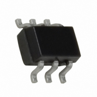
MOSFET N-CH 30V 2A SC70-6

FDG315N

Manufacturer Part Number
FDG315N
Description
MOSFET N-CH 30V 2A SC70-6
Manufacturer
Fairchild Semiconductor
Series
PowerTrench®r
Datasheet

Specifications of FDG315N

Fet Type
MOSFET N-Channel, Metal Oxide
Fet Feature
Logic Level Gate
Rds On (max) @ Id, Vgs
120 mOhm @ 2A, 10V
Drain To Source Voltage (vdss)
30V
Current - Continuous Drain (id) @ 25° C
2A
Vgs(th) (max) @ Id
3V @ 250µA
Gate Charge (qg) @ Vgs
4nC @ 5V
Input Capacitance (ciss) @ Vds
220pF @ 15V
Power - Max
480mW
Mounting Type
Surface Mount
Package / Case
SC-70-6, SC-88, SOT-363
Configuration
Single Quad Drain
Transistor Polarity
N-Channel
Resistance Drain-source Rds (on)
0.12 Ohm @ 10 V
Forward Transconductance Gfs (max / Min)
5 S
Drain-source Breakdown Voltage
30 V
Gate-source Breakdown Voltage
+/- 20 V
Continuous Drain Current
2 A
Power Dissipation
750 mW
Maximum Operating Temperature
+ 150 C
Mounting Style
SMD/SMT
Minimum Operating Temperature
- 55 C
Lead Free Status / RoHS Status
Lead free / RoHS Compliant
2000 Fairchild Semiconductor International
FDG315N
N-Channel Logic Level PowerTrench MOSFET
General Description
This N-Channel Logic Level MOSFET is produced using
Fairchild Semiconductor's advanced PowerTrench
process that has been especially tailored to minimize
on-state resistance and yet maintain superior switching
performance.
These devices are well suited for low voltage and
battery powered applications where low in-line power
loss and fast switching are required.
Applications
Absolute Maximum Ratings
V
V
I
P
T
Thermal Characteristics
R
Package Marking and Ordering Information
Symbol
D
J
DSS
GSS
D
DC/DC converter
Load switch
Power Management
, T
JA
Device Marking
stg
SC70-6
.
15
Drain-Source Voltage
Gate-Source Voltage
Drain Current
Power Dissipation for Single Operation
Operating and Storage Junction Temperature Range
Thermal Resistance, Junction-to-Ambient
D
D
S
D
- Continuous
- Pulsed
D
G
Parameter
FDG315N
Device
T
A
= 25°C unless otherwise noted
Reel Size
Features
7’’
(Note 1a)
(Note 1a)
(Note 1b)
(Note 1b)
2 A, 30 V. R
Low gate charge (2.1nC typical).
High performance trench technology for extremely low
Compact industry standard SC70-6 surface mount
package.
R
DS(ON)
.
R
DS(ON)
DS(ON)
2
1
3
3
Tape Width
= 0.12
= 0.16
-55 to +150
Ratings
8mm
0.75
0.48
260
30
20
2
6
@ V
@ V
GS
GS
6
= 10 V
5
4
= 4.5 V.
Quantity
3000 units
July 2000
Units
FDG315N Rev. C
C/W
W
V
V
A
C

Related parts for FDG315N

FDG315N Summary of contents

Page 1

... Compact industry standard SC70-6 surface mount package 25°C unless otherwise noted A Parameter (Note 1a) (Note 1a) (Note 1b) (Note 1b) Device Reel Size FDG315N 7’’ July 2000 = 0. DS(ON 0. 4.5 V. DS(ON Ratings Units 0.75 W 0.48 -55 to +150 C 260 C/W Tape Width Quantity 8mm 3000 units FDG315N Rev. C ...

Page 2

... Test Conditions 250 250 A, Referenced - 250 250 A, Referenced 125 1.0 MHz (Note GEN 0. determined by the user's board design. CA Min Typ Max Units mV 100 nA -100 mV/ C 0.100 0.12 0.140 0.20 0.130 0. 220 2 0.8 nC 0.7 nC 0.42 A 0.7 1.2 V (Note 2) FDG315N Rev ...

Page 3

... C 1 0.1 0.01 0.001 0 Figure 6. Body Diode Forward Voltage Variation with Source Current V = 3.5V GS 4.0V 4.5V 5.0V 6.0V 8.0V 10V DRAIN CURRENT ( 125 GATE TO SOURCE VOLTAGE ( 125 -55 C 0.4 0.6 0 BODY DIODE FORWARD VOLTAGE (V) SD and Temperature. FDG315N Rev 1.2 ...

Page 4

... Thermal characterization performed using the conditions described in Note 1b. Transient themal response will change depending on the circuit board design 1MHz ISS C OSS C RSS DRAIN TO SOURCE VOLTAGE (V) DS SINGLE PULSE 260 C 0.01 0 100 SINGLE PULSE TIME (SEC) Power Dissipation. R ( =260°C/W JA P(pk ( Duty Cycle 100 300 FDG315N Rev 1000 ...

Page 5

TRADEMARKS DISCLAIMER LIFE SUPPORT POLICY PRODUCT STATUS DEFINITIONS Definition of Terms Datasheet Identification Product Status Definition ...

Related keywords