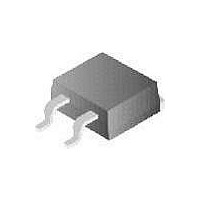
FDB20AN06A0 Fairchild Semiconductor, FDB20AN06A0 Datasheet - Page 5

FDB20AN06A0
Manufacturer Part Number
FDB20AN06A0
Description
MOSFET N-CH 60V 45A TO-263AB
Manufacturer
Fairchild Semiconductor
Series
PowerTrench®r
Datasheet
1.FDP20AN06A0.pdf
(11 pages)
Specifications of FDB20AN06A0
Fet Type
MOSFET N-Channel, Metal Oxide
Fet Feature
Standard
Rds On (max) @ Id, Vgs
20 mOhm @ 45A, 10V
Drain To Source Voltage (vdss)
60V
Current - Continuous Drain (id) @ 25° C
45A
Vgs(th) (max) @ Id
4V @ 250µA
Gate Charge (qg) @ Vgs
19nC @ 10V
Input Capacitance (ciss) @ Vds
950pF @ 25V
Power - Max
90W
Mounting Type
Surface Mount
Package / Case
D²Pak, TO-263 (2 leads + tab)
Configuration
Single
Transistor Polarity
N-Channel
Resistance Drain-source Rds (on)
0.017 Ohms @ 10 V
Drain-source Breakdown Voltage
60 V
Gate-source Breakdown Voltage
+/- 20 V
Continuous Drain Current
45 A
Power Dissipation
90 W
Maximum Operating Temperature
+ 175 C
Mounting Style
SMD/SMT
Minimum Operating Temperature
- 55 C
Lead Free Status / RoHS Status
Lead free / RoHS Compliant
©2003 Fairchild Semiconductor Corporation
Typical Characteristics
Figure 11. Normalized Gate Threshold Voltage vs
Figure 13. Capacitance vs Drain to Source
1000
2000
100
1.2
1.0
0.8
0.6
0.4
40
0.1
-80
V
C
GS
RSS
= 0V, f = 1MHz
-40
= C
Junction Temperature
V
GD
DS
T
J
, JUNCTION TEMPERATURE (
, DRAIN TO SOURCE VOLTAGE (V)
0
Voltage
1
40
80
V
T
GS
C
C
C
= 25°C unless otherwise noted
= V
ISS
OSS
120
10
DS
= C
o
≅ C
C)
, I
GS
D
DS
= 250µA
160
+ C
+ C
GD
GD
200
60
Figure 14. Gate Charge Waveforms for Constant
Breakdown Voltage vs Junction Temperature
10
8
6
4
2
0
1.15
1.10
1.05
1.00
0.95
0.90
Figure 12. Normalized Drain to Source
0
-80
V
DD
I
D
= 30V
= 250µA
-40
3
T
J
, JUNCTION TEMPERATURE (
Gate Current
Q
0
g
, GATE CHARGE (nC)
6
40
WAVEFORMS IN
DESCENDING ORDER:
80
9
FDB20AN06A0 / FDP20AN06A0 Rev. B
I
I
D
D
= 45A
= 9A
120
o
C)
12
160
200
15


