IPP100N04S2-04 Infineon Technologies, IPP100N04S2-04 Datasheet - Page 3
IPP100N04S2-04
Manufacturer Part Number
IPP100N04S2-04
Description
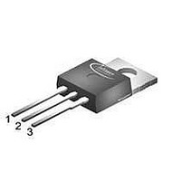
MOSFET N-CH 40V 100A TO220-3
Manufacturer
Infineon Technologies
Series
OptiMOS™r
Datasheet
1.IPB100N04S2-04.pdf
(8 pages)
Specifications of IPP100N04S2-04
Fet Type
MOSFET N-Channel, Metal Oxide
Fet Feature
Standard
Rds On (max) @ Id, Vgs
3.6 mOhm @ 80A, 10V
Drain To Source Voltage (vdss)
40V
Current - Continuous Drain (id) @ 25° C
100A
Vgs(th) (max) @ Id
4V @ 250µA
Gate Charge (qg) @ Vgs
172nC @ 10V
Input Capacitance (ciss) @ Vds
5300pF @ 25V
Power - Max
300W
Mounting Type
Through Hole
Package / Case
TO-220-3 (Straight Leads)
Configuration
Single
Transistor Polarity
N-Channel
Resistance Drain-source Rds (on)
3.6 m Ohms
Drain-source Breakdown Voltage
40 V
Gate-source Breakdown Voltage
+/- 20 V
Continuous Drain Current
100 A
Power Dissipation
300 W
Maximum Operating Temperature
+ 175 C
Mounting Style
Through Hole
Minimum Operating Temperature
- 55 C
Lead Free Status / RoHS Status
Lead free / RoHS Compliant
Other names
SP000219056
Available stocks
Company
Part Number
Manufacturer
Quantity
Price
Company:

Part Number:
IPP100N04S2-04
Manufacturer:
INFINEON
Quantity:
12 500


Rev. 1.0
1)
information see Application Note ANPS071E at www.infineon.com/optimos
2)
3)
4)
5)
connection. PCB is vertical in still air.
Parameter
Dynamic characteristics
Input capacitance
Output capacitance
Reverse transfer capacitance
Turn-on delay time
Rise time
Turn-off delay time
Fall time
Gate Charge Characteristics
Gate to source charge
Gate to drain charge
Gate charge total
Gate plateau voltage
Reverse Diode
Diode continous forward current
Diode pulse current
Diode forward voltage
Reverse recovery time
Reverse recovery charge
Current is limited by bondwire; with an R
Defined by design. Not subject to production test.
See diagram 13
Qualified at -20V and +20V.
Device on 40 mm x 40 mm x 1.5 mm epoxy PCB FR4 with 6 cm
2)
2)
2)
2)
2)
2)
Symbol
C
C
C
t
t
t
t
Q
Q
Q
V
I
I
V
t
Q
thJC
d(on)
r
d(off)
f
S
S,pulse
rr
rss
plateau
SD
iss
oss
gs
gd
g
rr
= 0.5K/W the chip is able to carry 210A at 25°C. For detailed
V
f =1 MHz
V
I
V
V
T
V
T
V
di
V
di
D
C
j
GS
DD
DD
GS
GS
R
R
=80 A, R
=25 °C
F
F
page 3
=25 °C
=20 V, I
=20 V, I
/dt =100 A/µs
/dt =100 A/µs
=0 V, V
=20 V, V
=32 V, I
=0 to 10 V
=0 V, I
Conditions
F
F
F
G
2
DS
=80 A,
=I
=I
D
=2.2
(one layer, 70 µm thick) copper area for drain
GS
=100 A,
=25 V,
S
S
=10 V,
,
,
min.
-
-
-
-
-
-
-
-
-
-
-
-
-
-
-
-
Values
5300
2200
typ.
580
125
153
4.9
0.9
27
46
56
33
26
46
66
-
-
IPB100N04S2-04
IPP100N04S2-04
max.
172
190
100
400
1.3
37
80
80
-
-
-
-
-
-
-
-
2006-03-02
Unit
pF
ns
nC
V
A
V
ns
nC
Related parts for IPP100N04S2-04
Image
Part Number
Description
Manufacturer
Datasheet
Request
R

Part Number:
Description:
Manufacturer:
Infineon Technologies AG
Datasheet:
Part Number:
Description:
Manufacturer:
Infineon Technologies AG
Datasheet:
Part Number:
Description:
Manufacturer:
Infineon Technologies AG
Datasheet:
Part Number:
Description:
Manufacturer:
Infineon Technologies AG
Datasheet:
Part Number:
Description:
Manufacturer:
Infineon Technologies AG
Datasheet:
Part Number:
Description:
Manufacturer:
Infineon Technologies AG
Datasheet:
Part Number:
Description:
Manufacturer:
Infineon Technologies AG
Datasheet:
Part Number:
Description:
16-bit microcontroller with 2x2 KByte RAM
Manufacturer:
Infineon Technologies AG
Datasheet:
Part Number:
Description:
NPN silicon RF transistor
Manufacturer:
Infineon Technologies AG
Datasheet:
Part Number:
Description:
NPN silicon RF transistor
Manufacturer:
Infineon Technologies AG
Datasheet:
Part Number:
Description:
NPN silicon RF transistor
Manufacturer:
Infineon Technologies AG
Datasheet:
Part Number:
Description:
NPN silicon RF transistor
Manufacturer:
Infineon Technologies AG
Datasheet:
Part Number:
Description:
Si-MMIC-amplifier in SIEGET 25-technologie
Manufacturer:
Infineon Technologies AG
Datasheet:
Part Number:
Description:
IGBT Power Module
Manufacturer:
Infineon Technologies AG
Datasheet:
Part Number:
Description:
IC for switching-mode power supplies
Manufacturer:
Infineon Technologies AG
Datasheet: