HRF3205 Fairchild Semiconductor, HRF3205 Datasheet - Page 2
HRF3205
Manufacturer Part Number
HRF3205
Description
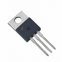
MOSFET N-CH 55V 100A TO-220AB
Manufacturer
Fairchild Semiconductor
Datasheet
1.HRF3205.pdf
(9 pages)
Specifications of HRF3205
Fet Type
MOSFET N-Channel, Metal Oxide
Fet Feature
Standard
Rds On (max) @ Id, Vgs
8 mOhm @ 59A, 10V
Drain To Source Voltage (vdss)
55V
Current - Continuous Drain (id) @ 25° C
100A
Vgs(th) (max) @ Id
4V @ 250µA
Gate Charge (qg) @ Vgs
170nC @ 10V
Input Capacitance (ciss) @ Vds
4000pF @ 25V
Power - Max
175W
Mounting Type
Through Hole
Package / Case
TO-220-3 (Straight Leads)
Lead Free Status / RoHS Status
Lead free / RoHS Compliant
Available stocks
Company
Part Number
Manufacturer
Quantity
Price
Company:

Part Number:
HRF3205
Manufacturer:
INTEL
Quantity:
5 240
Part Number:
HRF3205
Manufacturer:
FAIRCHILD/仙童
Quantity:
20 000


Absolute Maximum Ratings
Drain to Source Voltage (Note 1) . . . . . . . . . . . . . . . . . . . . . . . . . . . . . . . . . . . . . . . . . . . . V
Drain to Gate Voltage (R
Gate to Source Voltage . . . . . . . . . . . . . . . . . . . . . . . . . . . . . . . . . . . . . . . . . . . . . . . . . . . . V
Drain Current
Pulsed Avalanche Rating . . . . . . . . . . . . . . . . . . . . . . . . . . . . . . . . . . . . . . . . . . . . . . . . . . . E
Power Dissipation . . . . . . . . . . . . . . . . . . . . . . . . . . . . . . . . . . . . . . . . . . . . . . . . . . . . . . . . . P
Operating and Storage Temperature . . . . . . . . . . . . . . . . . . . . . . . . . . . . . . . . . . . . . . T
Maximum Temperature for Soldering
CAUTION: Stresses above those listed in “Absolute Maximum Ratings” may cause permanent damage to the device. This is a stress only rating and operation of the
device at these or any other conditions above those indicated in the operational sections of this specification is not implied.
NOTE:
Electrical Specifications
©2001 Fairchild Semiconductor Corporation
Drain to Source Breakdown Voltage
Gate to Source Threshold Voltage
Zero Gate Voltage Drain Current
Gate to Source Leakage Current
Breakdown Voltage Temperature
Coefficient
Drain to Source On Resistance
Turn-On Delay Time
Rise Time
Turn-Off Delay Time
Fall Time
Total Gate Charge
Gate to Source Charge
Gate to Drain “Miller” Charge
Input Capacitance
Output Capacitance
Reverse Transfer Capacitance
Internal Source Inductance
Internal Drain Inductance
Thermal Resistance Junction to Case
Thermal Resistance Junction to
Ambient
1. T
Continuous . . . . . . . . . . . . . . . . . . . . . . . . . . . . . . . . . . . . . . . . . . . . . . . . . . . . . . . . . . . . . I
Pulsed Drain Current (Note 2) . . . . . . . . . . . . . . . . . . . . . . . . . . . . . . . . . . . . . . . . . . . . . I
Derate Above 25
Leads at 0.063in (1.6mm) from Case for 10s . . . . . . . . . . . . . . . . . . . . . . . . . . . . . . . . . . . T
Package Body for 10s, See Techbrief 334 . . . . . . . . . . . . . . . . . . . . . . . . . . . . . . . . . . . T
J
= 25
o
C to 150
PARAMETER
o
C . . . . . . . . . . . . . . . . . . . . . . . . . . . . . . . . . . . . . . . . . . . . . . . . . . . . . . . .
o
C.
GS
= 20k ) (Note 1) . . . . . . . . . . . . . . . . . . . . . . . . . . . . . . . . V
T
C
= 25
T
C
SYMBOL
V
V
= 25
r
o
BV
t
DS(ON)
(BR)DSS
t
d(OFF)
C
C
GS(TH)
C, Unless Otherwise Specified
R
R
I
I
d(ON)
C
Q
GSS
Q
DSS
Q
OSS
L
RSS
L
ISS
DSS
T
t
t
gs
gd
r
S
D
f
JC
JA
o
g
J
C, Unless Othewise Specified
/
I
V
V
V
V
Reference to 25
I
V
R
R
V
V
(Figure 6)
V
f = 1MHz (Figure 5)
Measured From the Contact
Screw on Tab to Center of Die
Measured From the Drain
Lead, 6mm (0.25in) From
Package to Center of Die
Measured From the Source
Lead, 6mm (0.25in) From Head-
er to Source Bonding Pad
TO-220
TO-263 (PCB Mount, Steady State)
D
D
GS
DS
DS
GS
DD
L
GS
DD
GS
DS
= 250 A, V
= 59A, V
= 0.47 , V
= V
= 55V, V
= 44V, V
= 20V
= 28V, I
= 44V, I
= 10V, I
= 25V, V
= 2.5
DS
, I
GS
D
D
g(REF)
D
GS
GS
GS
GS
GS
= 10V (Figure 4)
= 250 A
o
TEST CONDITIONS
59A,
59A,
C, I
= 0V
= 0V, T
= 0V,
= 0V
10V,
= 3mA
D
= 250 A
C
= 150
J
, T
Modified MOSFET
Symbol Showing the
Internal Devices In-
ductances
o
G
DGR
C
DSS
STG
pkg
DM
GS
AS
D
D
L
L
L
D
S
D
S
MIN
-55 to 175
55
Figure 10
2
-
-
-
-
-
-
-
-
-
-
-
-
-
-
-
-
-
-
-
-
1.17
100
390
175
300
260
20V
55
55
0.0065
0.057
4000
1300
TYP
100
480
7.5
4.5
14
43
70
-
-
-
-
-
-
-
-
-
-
-
HRF3205, HRF3205S Rev. B
0.008
MAX
0.85
250
100
170
25
32
74
62
40
4
-
-
-
-
-
-
-
-
-
-
-
W/
UNITS
o
o
o
o
o
o
W
V
V
V
A
A
C/W
C/W
C/W
nC
nC
nC
nH
nH
C
C
C
nA
pF
pF
pF
o
ns
ns
ns
ns
V
V
V
A
A
C
Related parts for HRF3205
Image
Part Number
Description
Manufacturer
Datasheet
Request
R

Part Number:
Description:
Fairchild Semiconductor [IGBT MODULE]
Manufacturer:
Fairchild Semiconductor
Datasheet:

Part Number:
Description:
Discrete Semiconductor Modules
Manufacturer:
Fairchild Semiconductor
Part Number:
Description:
Discrete Semiconductor Modules
Manufacturer:
Fairchild Semiconductor
Part Number:
Description:
This N-Channel MOSFET is produced using Fairchild Semiconductor’s advanced Power Trench® process
Manufacturer:
Fairchild Semiconductor
Datasheet:
Part Number:
Description:
This N-Channel MOSFET is produced using Fairchild Semiconductor’s advanced Power Trench® process
Manufacturer:
Fairchild Semiconductor
Datasheet:
Part Number:
Description:
This N-Channel MOSFET is produced using Fairchild Semiconductor’s advanced PowerTrench® process
Manufacturer:
Fairchild Semiconductor
Datasheet:
Part Number:
Description:
This N-Channel MOSFET is produced using Fairchild Semiconductor’s advanced PowerTrench® process
Manufacturer:
Fairchild Semiconductor
Datasheet:
Part Number:
Description:
This N-Channel MOSFET is produced using Fairchild Semiconductor’s advanced Power Trench® process
Manufacturer:
Fairchild Semiconductor
Datasheet:
Part Number:
Description:
This N-Channel logic Level MOSFETs are produced using Fairchild Semiconductor‘s advanced Power Trench® process that has been special tailored to minimize the on-state resistance and yet maintain superior switching performance
Manufacturer:
Fairchild Semiconductor
Datasheet:
Part Number:
Description:
This N-Channel MOSFET is produced using Fairchild Semiconductor’s advanced Power Trench® process
Manufacturer:
Fairchild Semiconductor
Datasheet:
Part Number:
Description:
This N-Channel SyncFET™ is produced using Fairchild Semiconductor’s advanced PowerTrench® process
Manufacturer:
Fairchild Semiconductor
Datasheet:
Part Number:
Description:
This N-Channel SyncFET™ is produced using Fairchild Semiconductor’s advanced PowerTrench® process
Manufacturer:
Fairchild Semiconductor
Datasheet:
Part Number:
Description:
This N-Channel SyncFET™ is produced using Fairchild Semiconductor’s advanced PowerTrench® process
Manufacturer:
Fairchild Semiconductor
Datasheet:
Part Number:
Description:
This N-Channel logic Level MOSFETs are produced using Fairchild Semiconductor‘s advanced Power Trench® process that has been special tailored to minimize the on-state resistance and yet maintain superior switching performance
Manufacturer:
Fairchild Semiconductor
Datasheet:
Part Number:
Description:
This N-Channel MOSFET is produced using Fairchild Semiconductor’s advanced Power Trench® process that has been especially tailored to minimize the on-state resistance and yet maintain superior switching performance
Manufacturer:
Fairchild Semiconductor
Datasheet: