HUFA76429S3ST Fairchild Semiconductor, HUFA76429S3ST Datasheet
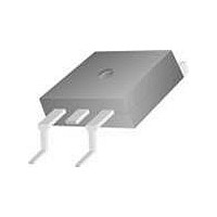
MOSFET N-CH 60V 47A D2PAK

HUFA76429S3ST

Manufacturer Part Number
HUFA76429S3ST
Description
MOSFET N-CH 60V 47A D2PAK
Manufacturer
Fairchild Semiconductor
Series
UltraFET™r
Datasheet

Specifications of HUFA76429S3ST

Fet Type
MOSFET N-Channel, Metal Oxide
Fet Feature
Logic Level Gate
Rds On (max) @ Id, Vgs
22 mOhm @ 47A, 10V
Drain To Source Voltage (vdss)
60V
Current - Continuous Drain (id) @ 25° C
47A
Vgs(th) (max) @ Id
3V @ 250µA
Gate Charge (qg) @ Vgs
46nC @ 10V
Input Capacitance (ciss) @ Vds
1480pF @ 25V
Power - Max
110W
Mounting Type
Surface Mount
Package / Case
D²Pak, TO-263 (2 leads + tab)
Configuration
Single
Transistor Polarity
N-Channel
Resistance Drain-source Rds (on)
0.018 Ohms
Drain-source Breakdown Voltage
60 V
Gate-source Breakdown Voltage
+/- 16 V
Continuous Drain Current
44 A
Power Dissipation
110 W
Maximum Operating Temperature
+ 175 C
Mounting Style
SMD/SMT
Fall Time
74 ns, 104 ns
Minimum Operating Temperature
- 55 C
Rise Time
203 ns, 100 ns
Lead Free Status / RoHS Status
Lead free / RoHS Compliant
©2001 Fairchild Semiconductor Corporation
20A, 60V, 0.027 Ohm, N-Channel, Logic
Level UltraFET® Power MOSFETs
Packaging
Symbol
Absolute Maximum Ratings
Drain to Source Voltage (Note 1) . . . . . . . . . . . . . . . . . . . . . . . . . . . . . . . . . . . . . . . . . . . . . . . V
Drain to Gate Voltage (R
Gate to Source Voltage . . . . . . . . . . . . . . . . . . . . . . . . . . . . . . . . . . . . . . . . . . . . . . . . . . . . . . . V
Drain Current
Pulsed Avalanche Rating . . . . . . . . . . . . . . . . . . . . . . . . . . . . . . . . . . . . . . . . . . . . . . . . . . . . . .UIS
Power Dissipation . . . . . . . . . . . . . . . . . . . . . . . . . . . . . . . . . . . . . . . . . . . . . . . . . . . . . . . . . . . . P
Operating and Storage Temperature . . . . . . . . . . . . . . . . . . . . . . . . . . . . . . . . . . . . . . . . . T
Maximum Temperature for Soldering
NOTES:
CAUTION: Stresses above those listed in “Absolute Maximum Ratings” may cause permanent damage to the device. This is a stress only rating and operation of the
device at these or any other conditions above those indicated in the operational sections of this specification is not implied.
This product has been designed to meet the extreme test conditions and environment demanded by the automotive industry. For a copy
All Fairchild semiconductor products are manufactured, assembled and tested under ISO9000 and QS9000 quality systems certification.
1. T
Continuous (T
Continuous (T
Continuous (T
Continuous (T
Pulsed Drain Current . . . . . . . . . . . . . . . . . . . . . . . . . . . . . . . . . . . . . . . . . . . . . . . . . . . . . . . .I
Derate Above 25
Leads at 0.063in (1.6mm) from Case for 10s. . . . . . . . . . . . . . . . . . . . . . . . . . . . . . . . . . . . . . .T
Package Body for 10s, See Techbrief TB334 . . . . . . . . . . . . . . . . . . . . . . . . . . . . . . . . . . . . . T
(FLANGE)
DRAIN
J
= 25
JEDEC TO-251AA
HUFA76429D3
o
C to 150
C
C
C
C
= 25
= 25
= 100
= 100
o
C . . . . . . . . . . . . . . . . . . . . . . . . . . . . . . . . . . . . . . . . . . . . . . . . . . . . . . . . . . . .
o
SOURCE
o
o
C.
C, V
C, V
o
o
DRAIN
GS
C, V
C, V
G
GATE
GS
GS
= 20k Ω ) (Note 1) . . . . . . . . . . . . . . . . . . . . . . . . . . . . . . . . . . . . . V
GS
GS
Reliability data can be found at: http://www.mtp.fairchild.com/automotive.html.
= 5V) . . . . . . . . . . . . . . . . . . . . . . . . . . . . . . . . . . . . . . . . . . . . . . I
= 10V) (Figure 2) . . . . . . . . . . . . . . . . . . . . . . . . . . . . . . . . . . . . . I
= 5V) . . . . . . . . . . . . . . . . . . . . . . . . . . . . . . . . . . . . . . . . . . . . . I
= 4.5V) (Figure 2) . . . . . . . . . . . . . . . . . . . . . . . . . . . . . . . . . . . I
D
S
SOURCE
of the requirements, see AEC Q101 at: http://www.aecouncil.com/
GATE
T
Data Sheet
C
JEDEC TO-252AA
HUFA76429D3S
= 25
o
C, Unless Otherwise Specified
(FLANGE)
DRAIN
HUFA76429D3, HUFA76429D3S
Features
• Ultra Low On-Resistance
• Simulation Models
• Peak Current vs Pulse Width Curve
• UIS Rating Curve
• Switching Time vs R
Ordering Information
NOTE: When ordering, use the entire part number. Add the suffix T
to obtain the variant in tape and reel, e.g., HUFA76429D3ST.
HUFA76429D3
HUFA76429D3S
- r
- r
- Temperature Compensated PSPICE® and SABER™
- Spice and SABER Thermal Impedance Models
- www.fairchild.com
PART NUMBER
Electriecal Models
DS(ON)
DS(ON)
December 2001
J
, T
= 0.023 Ω,
= 0.027 Ω,
DGR
DSS
STG
pkg
DM
GS
D
D
D
D
D
L
HUFA76429D3, HUFA76429D3S
TO-251AA
TO-252AA
GS
V
V
PACKAGE
GS
GS
Figures 6, 17, 18
Curves
= 10V
= 5V
-55 to 175
Figure 4
0.74
± 16
110
300
260
60
60
20
20
20
20
HUFA76429D3, HUFA76429D3S Rev. B
76429D
76429D
BRAND
UNITS
W/
o
o
o
W
V
V
V
A
A
A
A
C
C
C
o
C

Related parts for HUFA76429S3ST

HUFA76429S3ST Summary of contents

Page 1

... This product has been designed to meet the extreme test conditions and environment demanded by the automotive industry. For a copy of the requirements, see AEC Q101 at: http://www.aecouncil.com/ Reliability data can be found at: http://www.mtp.fairchild.com/automotive.html. All Fairchild semiconductor products are manufactured, assembled and tested under ISO9000 and QS9000 quality systems certification. ©2001 Fairchild Semiconductor Corporation HUFA76429D3, HUFA76429D3S ...

Page 2

... CAPACITANCE SPECIFICATIONS Input Capacitance Output Capacitance Reverse Transfer Capacitance Source to Drain Diode Specifications PARAMETER Source to Drain Diode Voltage Reverse Recovery Time Reverse Recovered Charge ©2001 Fairchild Semiconductor Corporation o C, Unless Otherwise Specified SYMBOL TEST CONDITIONS = 250 µ (Figure 12) ...

Page 3

... SINGLE PULSE 0. FIGURE 3. NORMALIZED MAXIMUM TRANSIENT THERMAL IMPEDANCE 600 V = 10V GS 100 TRANSCONDUCTANCE MAY LIMIT CURRENT IN THIS REGION ©2001 Fairchild Semiconductor Corporation 150 175 25 125 o C) FIGURE 2. MAXIMUM CONTINUOUS DRAIN CURRENT RECTANGULAR PULSE DURATION ( PULSE WIDTH (s) FIGURE 4. PEAK CURRENT CAPABILITY ...

Page 4

... FIGURE 7. TRANSFER CHARACTERISTICS 20A 10A GATE TO SOURCE VOLTAGE (V) GS FIGURE 9. DRAIN TO SOURCE ON RESISTANCE vs GATE VOLTAGE AND DRAIN CURRENT ©2001 Fairchild Semiconductor Corporation (Continued) 100 100µs 1ms 10ms 100 NOTE: Refer to Fairchild Application Notes AN9321 and AN9322. FIGURE 6. UNCLAMPED INDUCTIVE SWITCHING - ...

Page 5

... FIGURE 13. CAPACITANCE vs DRAIN TO SOURCE VOLTAGE 400 V = 4.5V 30V 20A 300 t r 200 t f 100 GATE TO SOURCE RESISTANCE (Ω) GS FIGURE 15. SWITCHING TIME vs GATE RESISTANCE ©2001 Fairchild Semiconductor Corporation (Continued 250µ 120 160 200 o C) FIGURE 12. NORMALIZED DRAIN TO SOURCE BREAKDOWN 0V 1MHz ISS GS GD ≅ ...

Page 6

... Test Circuits and Waveforms VARY t TO OBTAIN P R REQUIRED PEAK FIGURE 17. UNCLAMPED ENERGY TEST CIRCUIT g(REF) FIGURE 19. GATE CHARGE TEST CIRCUIT FIGURE 21. SWITCHING TIME TEST CIRCUIT ©2001 Fairchild Semiconductor Corporation DUT 0.01Ω DUT g(REF DUT DSS FIGURE 18. UNCLAMPED ENERGY WAVEFORMS ...

Page 7

... NOTE: For further discussion of the PSPICE model, consult A New PSPICE Sub-Circuit for the Power MOSFET Featuring Global Temperature Options; IEEE Power Electronics Specialist Conference Records, 1991, written by William J. Hepp and C. Frank Wheatley. ©2001 Fairchild Semiconductor Corporation rev 5 July 1999 DPLCAP ...

Page 8

... Fairchild Semiconductor Corporation DPLCAP 10 RSLC2 - 6 ESG 8 EVTHRES + ...

Page 9

... Fairchild Semiconductor Corporation JUNCTION th RTHERM1 CTHERM1 6 RTHERM2 CTHERM2 5 RTHERM3 CTHERM3 4 RTHERM4 CTHERM4 3 RTHERM5 ...

Page 10

... TRADEMARKS The following are registered and unregistered trademarks Fairchild Semiconductor owns or is authorized to use and is not intended exhaustive list of all such trademarks. ACEx™ FAST Bottomless™ FASTr™ FRFET™ CoolFET™ GlobalOptoisolator™ CROSSVOLT™ GTO™ DenseTrench™ ...

Related keywords