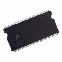
MT46V64M8P-5B:F Micron Technology Inc, MT46V64M8P-5B:F Datasheet - Page 12

MT46V64M8P-5B:F
Manufacturer Part Number
MT46V64M8P-5B:F
Description
DRAM Chip DDR SDRAM 512M-Bit 64Mx8 2.6V 66-Pin TSOP Tray
Manufacturer
Micron Technology Inc
Type
DDR SDRAMr
Datasheet
1.MT46V32M16P-5BF_TR.pdf
(91 pages)
Specifications of MT46V64M8P-5B:F
Density
512 Mb
Maximum Clock Rate
400 MHz
Package
66TSOP
Address Bus Width
15 Bit
Operating Supply Voltage
2.6 V
Maximum Random Access Time
0.7 ns
Operating Temperature
0 to 70 °C
Format - Memory
RAM
Memory Type
DDR SDRAM
Memory Size
512M (64M x 8)
Speed
5ns
Interface
Parallel
Voltage - Supply
2.5 V ~ 2.7 V
Package / Case
66-TSOP
Organization
64Mx8
Address Bus
15b
Access Time (max)
700ps
Operating Supply Voltage (typ)
2.6V
Package Type
TSOP
Operating Temp Range
0C to 70C
Operating Supply Voltage (max)
2.7V
Operating Supply Voltage (min)
2.5V
Supply Current
195mA
Pin Count
66
Mounting
Surface Mount
Operating Temperature Classification
Commercial
Lead Free Status / RoHS Status
Lead free / RoHS Compliant
Available stocks
Company
Part Number
Manufacturer
Quantity
Price
Company:
Part Number:
MT46V64M8P-5B:F
Manufacturer:
MICRON
Quantity:
3 400
Company:
Part Number:
MT46V64M8P-5B:F
Manufacturer:
MICRON
Quantity:
2 526
Part Number:
MT46V64M8P-5B:F
Manufacturer:
MICRON/美光
Quantity:
20 000
Table 4:
Table 5:
PDF: 09005aef80a1d9d4/Source: 09005aef82a95a3a
512Mb_DDR_x4x8x16_D2.fm - 512Mb DDR: Rev. N; Core DDR Rev. B 2/09 EN
C9, D1, D9,
C9, D1, D9,
A2, A8, C3,
F8, M7, A7
B2, D2, C8,
A3, F2, M3
A1, C2, E2,
B1, B9, C1,
B1, B9, C1,
Numbers
E1, E7, E9,
E1, E7, E9,
B8, D8
E8, A9
FBGA
Numbers
C7
E3
E7
E3
F1
F7
F7
F9
TSOP
–
17
3, 9, 15, 55,
4, 7, 10, 13,
2, 8, 59, 65
Pin and Ball Descriptions (continued)
Reserved NC Pin and Ball Descriptions
NC pins not listed may also be reserved for other uses; this table defines NC pins of importance
14, 17, 25,
13, 14, 16,
17, 20, 25,
43, 53, 54,
14, 16, 17,
20, 25, 43,
53, 54, 57,
Numbers
34, 48, 66
57, 60, 63
6, 12, 52,
1, 18, 33
4, 7, 10,
58, 64
43, 53
60, 63
TSOP
19, 50
51
16
51
61
49
Symbol
A13
Symbol
UDQS
V
LDQS
V
DNU
DQS
V
V
V
NC
NC
NC
DD
NF
SS
REF
DD
SS
Q
Q
Input
Type
Supply Power supply: +2.5V ±0.2V. (+2.6V ±0.1V for DDR400).
Supply DQ power supply: +2.5V ±0.2V (+2.6V ±0.1V for DDR400). Isolated on
Supply SSTL_2 reference voltage.
Supply Ground.
Supply DQ ground: Isolated on the die for improved noise immunity.
Type
I/O
–
–
–
–
–
Description
Description
Data strobe: Output with read data, input with write data. DQS is edge-
aligned with read data, centered in write data. It is used to capture data.
For the x16, LDQS is DQS for DQ0–DQ7 and UDQS is DQS for DQ8–DQ15.
Pin 16 (E7) is NC on x4 and x8.
the die for improved noise immunity.
No connect for x16: These pins should be left unconnected.
No connect for x8: These pins should be left unconnected.
No connect for x4: These pins should be left unconnected.
No function for x4: These pins should be left unconnected.
Do not use: Must float to minimize noise on V
Address input A13 for 1Gb devices.
12
Pin and Ball Assignments and Descriptions
Micron Technology, Inc., reserves the right to change products or specifications without notice.
512Mb: x4, x8, x16 DDR SDRAM
©2000 Micron Technology, Inc. All rights reserved.
REF
.


