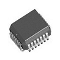
IDT82V1671J IDT, Integrated Device Technology Inc, IDT82V1671J Datasheet - Page 22

IDT82V1671J
Manufacturer Part Number
IDT82V1671J
Description
Manufacturer
IDT, Integrated Device Technology Inc
Datasheet
1.IDT82V1671J.pdf
(107 pages)
Specifications of IDT82V1671J
Number Of Channels
4
On-hook Transmission
Yes
Polarity Reversal
Yes
On-chip Ring Relay Driver
Yes
Operating Supply Voltage (typ)
3.3V
Operating Temp Range
-40C to 85C
Package Type
PLCC
Operating Temperature Classification
Industrial
Pin Count
28
Mounting
Surface Mount
Operating Current
95mA
Operating Supply Voltage (max)
3.465V
Operating Supply Voltage (min)
3.135V
Lead Free Status / RoHS Status
Not Compliant
Available stocks
Company
Part Number
Manufacturer
Quantity
Price
Company:
Part Number:
IDT82V1671J
Manufacturer:
BROADCOM
Quantity:
457
Part Number:
IDT82V1671J
Manufacturer:
IDT
Quantity:
20 000
Ω, as selected by the IM_629 bit in register LREG7. The option of
AGIS=600 Ω is only applicable to loops with 600 Ω equivalent
impedance, while the option of AGIS=900 Ω is applicable to all loops
including those with 600 Ω equivalent impedance. The AGIS value is set
to 600 Ω by default.
Impedance Scaling in the Coe-RAM. It is programmable from −128 to
+127 at increment of 1. The default value is 0.
bit is set to 0, the Impedance Matching Filter Coefficient in the Coe-RAM
is used by the IMF filter. Refer to
Coefficient RAM Mapping.
3.3.2.2
balance filter (ECF) for each channel to improve 4-wire return loss
performance. The ECF coefficient is programmable. If the ECF bit in
register LREG4 is set to 1, the ECF filter is disabled. If the ECF bit is set
to 0, the Transhybrid Balance Filter Coefficient in the Coe-RAM is used.
3.3.2.3
the frequency distortion caused by the impedance matching filter. The
RSLIC & CODEC CHIPSET
The analog gain for impedance scaling (AGIS) can be 600 Ω or 900
The coefficient for the GIS filter is programmed by Gain for
If the IMF bit in LREG4 is set to 1, the IMF filter is disabled. If the IMF
The RSLIC-CODEC chipset provides a traditional transhybrid
The frequency response correction filters are used to compensate for
Transhybrid Balance
Frequency Response Correction
Table - 23 on page 62
for the
22
chipset provides two frequency response correction filters per channel:
one is in the transmit path (FRX), the other is in the receive path (FRR).
or programmed by the Coe-RAM. If the FRX bit is set to 1, the FRX filter
is disabled. If the FRX bit is set to 0, the Coefficient for Frequency
Response Correction in the Transmit Path in the Coe-RAM is used.
or programmed by the Coe-RAM. If the FRR bit is set to 1, the FRR filter
is disabled. If the FRR bit is set to 0, the Coefficient for Frequency
Response Correction in the Receive Path in the Coe-RAM is used.
3.3.2.4
programming the digital filter GTX. The transmit gain can be up to +12
dB in minimum steps of 0.05 dB. If the GTX bit in LREG4 is set to 1, the
default transmit gain of 0 dB is selected. If the GTX bit is set to 0, the
transmit gain is programmed via the Coe-RAM.
gain and digital gain (GRX). The analog gain is fixed at 0 dB. The digital
gain is programmable from −12 dB to +3 dB in minimum steps of 0.05
dB. If the GRX bit in LREG4 is set to 1, the digital gain in the receive
path will be 0 dB (default value), otherwise, it is programmed via the
Coe-RAM.
The FRX bit in LREG4 determines whether the FRX filter is disabled
The FRR bit in LREG4 determines whether the FRR filter is disabled
For each channel, the gain in the transmit path is adjusted by
For each channel, the gain in the receive path consists of analog
Gain Adjustment
IDT82V1671/IDT82V1671A, IDT82V1074


