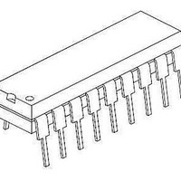
PIC16LF1847-E/ML Microchip Technology, PIC16LF1847-E/ML Datasheet - Page 280

PIC16LF1847-E/ML
Manufacturer Part Number
PIC16LF1847-E/ML
Description
14 KB Flash, 1K Bytes RAM, 32 MHz Int. Osc, 16 I/0, Enhanced Mid Range Core, Nan
Manufacturer
Microchip Technology
Series
PIC® XLP™ mTouch™ 16Fr
Datasheet
1.PIC16F1847-EP.pdf
(408 pages)
Specifications of PIC16LF1847-E/ML
Core Processor
PIC
Core Size
8-Bit
Speed
32MHz
Connectivity
I²C, LIN, SPI, UART/USART
Peripherals
Brown-out Detect/Reset, POR, PWM, WDT
Number Of I /o
15
Program Memory Size
14KB (8K x 14)
Program Memory Type
FLASH
Eeprom Size
256 x 8
Ram Size
1K x 8
Voltage - Supply (vcc/vdd)
1.8 V ~ 3.6 V
Data Converters
A/D 12x10b
Oscillator Type
Internal
Operating Temperature
-40°C ~ 125°C
Package / Case
28-VQFN Exposed Pad
Core
PIC
Processor Series
PIC16LF
Data Bus Width
8 bit
Maximum Clock Frequency
32 MHz
Data Ram Size
256 B
Number Of Programmable I/os
15
Number Of Timers
ÿ4 x 8-bit, 1 x 16-bit
Operating Supply Voltage
1.8 V to 5.5 V
Mounting Style
Through Hole
Interface Type
SPI, I2C
Lead Free Status / Rohs Status
Lead free / RoHS Compliant
- Current page: 280 of 408
- Download datasheet (4Mb)
PIC16(L)F1847
25.7
The MSSPx module has a Baud Rate Generator avail-
able for clock generation in both I
modes. The Baud Rate Generator (BRG) reload value
is placed in the SSPxADD register
When a write occurs to SSPxBUF, the Baud Rate Gen-
erator will automatically begin counting down.
Once the given operation is complete, the internal clock
will automatically stop counting and the clock pin will
remain in its last state.
An internal signal “Reload” in
value from SSPxADD to be loaded into the BRG
counter. This occurs twice for each oscillation of the
FIGURE 25-40:
TABLE 25-4:
25.7.1
This module incorporates I/O pins that can be moved to
other locations with the use of the alternate pin function
registers, APFCON0 and APFCON1. To determine
which pins can be moved and what their default loca-
tions are upon a Reset, see
Pin Function”
DS41453B-page 280
Note 1:
Note: Values of 0x00, 0x01 and 0x02 are not valid
Baud Rate Generator
for SSPxADD when used as a Baud Rate
Generator for I
limitation.
32 MHz
32 MHz
32 MHz
16 MHz
16 MHz
16 MHz
4 MHz
The I
100 kHz) in all details, but may be used with care where higher rates are required by the application.
ALTERNATE PIN LOCATIONS
F
OSC
for more information.
2
C interface does not conform to the 400 kHz I
MSSPX CLOCK RATE W/BRG
BAUD RATE GENERATOR BLOCK DIAGRAM
2
C. This is an implementation
SSPM<3:0>
Section 12.1 “Alternate
Figure 25-39
SCLx
2
C and SPI Master
(Register
8 MHz
8 MHz
8 MHz
4 MHz
4 MHz
4 MHz
1 MHz
SSPM<3:0>
F
triggers the
CY
Control
Reload
25-6).
SSPxCLK
Preliminary
Reload
2
module clock line. The logic dictating when the reload
signal is asserted depends on the mode the MSSPx is
being operated in.
Table 25-4
instruction cycles and the BRG value loaded into
SSPxADD.
EQUATION 25-1:
C specification (which applies to rates greater than
BRG Down Counter
SSPxADD<7:0>
BRG Value
0Ch
13h
19h
4Fh
09h
27h
09h
F
CLOCK
demonstrates clock rates based on
=
-------------------------------------------------
2011 Microchip Technology Inc.
SSPxADD
F
OSC
(2 Rollovers of BRG)
/2
F
OSC
400 kHz
400 kHz
308 kHz
100 kHz
308 kHz
100 kHz
100 kHz
F
+
CLOCK
1
4
(1)
(1)
Related parts for PIC16LF1847-E/ML
Image
Part Number
Description
Manufacturer
Datasheet
Request
R

Part Number:
Description:
IC, 8BIT MCU, PIC16LF, 32MHZ, QFN-28
Manufacturer:
Microchip Technology
Datasheet:

Part Number:
Description:
IC, 8BIT MCU, PIC16LF, 32MHZ, QFN-28
Manufacturer:
Microchip Technology
Datasheet:

Part Number:
Description:
IC, 8BIT MCU, PIC16LF, 32MHZ, DIP-18
Manufacturer:
Microchip Technology
Datasheet:

Part Number:
Description:
IC, 8BIT MCU, PIC16LF, 20MHZ, TQFP-44
Manufacturer:
Microchip Technology
Datasheet:

Part Number:
Description:
7 KB Flash, 384 Bytes RAM, 32 MHz Int. Osc, 16 I/0, Enhanced Mid Range Core, Nan
Manufacturer:
Microchip Technology

Part Number:
Description:
14KB Flash, 512B RAM, LCD, 11x10b ADC, EUSART, NanoWatt XLP 28 SOIC .300in T/R
Manufacturer:
Microchip Technology
Datasheet:

Part Number:
Description:
14KB Flash, 512B RAM, LCD, 11x10b ADC, EUSART, NanoWatt XLP 28 SSOP .209in T/R
Manufacturer:
Microchip Technology
Datasheet:

Part Number:
Description:
MCU PIC 14KB FLASH XLP 28-SSOP
Manufacturer:
Microchip Technology

Part Number:
Description:
MCU PIC 14KB FLASH XLP 28-SOIC
Manufacturer:
Microchip Technology

Part Number:
Description:
MCU PIC 512B FLASH XLP 28-UQFN
Manufacturer:
Microchip Technology

Part Number:
Description:
MCU PIC 14KB FLASH XLP 28-SPDIP
Manufacturer:
Microchip Technology

Part Number:
Description:
MCU 7KB FLASH 256B RAM 40-UQFN
Manufacturer:
Microchip Technology

Part Number:
Description:
MCU 7KB FLASH 256B RAM 44-TQFP
Manufacturer:
Microchip Technology

Part Number:
Description:
MCU 14KB FLASH 1KB RAM 28-UQFN
Manufacturer:
Microchip Technology

Part Number:
Description:
MCU PIC 14KB FLASH XLP 40-UQFN
Manufacturer:
Microchip Technology


