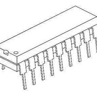
PIC16LF1847-E/ML Microchip Technology, PIC16LF1847-E/ML Datasheet - Page 283

PIC16LF1847-E/ML
Manufacturer Part Number
PIC16LF1847-E/ML
Description
14 KB Flash, 1K Bytes RAM, 32 MHz Int. Osc, 16 I/0, Enhanced Mid Range Core, Nan
Manufacturer
Microchip Technology
Series
PIC® XLP™ mTouch™ 16Fr
Datasheet
1.PIC16F1847-EP.pdf
(408 pages)
Specifications of PIC16LF1847-E/ML
Core Processor
PIC
Core Size
8-Bit
Speed
32MHz
Connectivity
I²C, LIN, SPI, UART/USART
Peripherals
Brown-out Detect/Reset, POR, PWM, WDT
Number Of I /o
15
Program Memory Size
14KB (8K x 14)
Program Memory Type
FLASH
Eeprom Size
256 x 8
Ram Size
1K x 8
Voltage - Supply (vcc/vdd)
1.8 V ~ 3.6 V
Data Converters
A/D 12x10b
Oscillator Type
Internal
Operating Temperature
-40°C ~ 125°C
Package / Case
28-VQFN Exposed Pad
Core
PIC
Processor Series
PIC16LF
Data Bus Width
8 bit
Maximum Clock Frequency
32 MHz
Data Ram Size
256 B
Number Of Programmable I/os
15
Number Of Timers
ÿ4 x 8-bit, 1 x 16-bit
Operating Supply Voltage
1.8 V to 5.5 V
Mounting Style
Through Hole
Interface Type
SPI, I2C
Lead Free Status / Rohs Status
Lead free / RoHS Compliant
- Current page: 283 of 408
- Download datasheet (4Mb)
REGISTER 25-3:
2011 Microchip Technology Inc.
bit 7
Legend:
R = Readable bit
u = Bit is unchanged
‘1’ = Bit is set
bit 7
bit 6
bit 5
bit 4
bit 3
bit 2
bit 1
bit 0
Note 1:
R/W-0/0
GCEN
For bits ACKEN, RCEN, PEN, RSEN, SEN: If the I
set (no spooling) and the SSPxBUF may not be written (or writes to the SSPxBUF are disabled).
GCEN: General Call Enable bit (in I
1 = Enable interrupt when a general call address (0x00 or 00h) is received in the SSPxSR
0 = General call address disabled
ACKSTAT: Acknowledge Status bit (in I
1 = Acknowledge was not received
0 = Acknowledge was received
ACKDT: Acknowledge Data bit (in I
In Receive mode:
Value transmitted when the user initiates an Acknowledge sequence at the end of a receive
1 = Not Acknowledge
0 = Acknowledge
ACKEN: Acknowledge Sequence Enable bit (in I
In Master Receive mode:
1 = Initiate Acknowledge sequence on SDAx and SCLx pins, and transmit ACKDT data bit.
0 = Acknowledge sequence idle
RCEN: Receive Enable bit (in I
1 = Enables Receive mode for I
0 = Receive idle
PEN: Stop Condition Enable bit (in I
SCKx Release Control:
1 = Initiate Stop condition on SDAx and SCLx pins. Automatically cleared by hardware.
0 = Stop condition Idle
RSEN: Repeated Start Condition Enabled bit (in I
1 = Initiate Repeated Start condition on SDAx and SCLx pins. Automatically cleared by hardware.
0 = Repeated Start condition Idle
SEN: Start Condition Enabled bit (in I
In Master mode:
1 = Initiate Start condition on SDAx and SCLx pins. Automatically cleared by hardware.
0 = Start condition Idle
In Slave mode:
1 = Clock stretching is enabled for both slave transmit and slave receive (stretch enabled)
0 = Clock stretching is disabled
ACKSTAT
R-0/0
Automatically cleared by hardware.
SSPxCON2: SSPx CONTROL REGISTER 2
W = Writable bit
x = Bit is unknown
‘0’ = Bit is cleared
R/W-0/0
ACKDT
R/S/HS-0/0
2
ACKEN
2
C Master mode only)
C
Preliminary
2
2
2
C mode only)
C Slave mode only)
C Master mode only)
2
C Master mode only)
2
C mode only)
U = Unimplemented bit, read as ‘0’
-n/n = Value at POR and BOR/Value at all other Resets
HC = Cleared by hardware
R/S/HS-0/0
2
RCEN
C module is not in the Idle mode, this bit may not be
2
2
C Master mode only)
C Master mode only)
R/S/HS-0/0
PEN
PIC16(L)F1847
S = User set
R/S/HS-0/0
RSEN
DS41453B-page 283
R/W/HS-0/0
SEN
bit 0
Related parts for PIC16LF1847-E/ML
Image
Part Number
Description
Manufacturer
Datasheet
Request
R

Part Number:
Description:
IC, 8BIT MCU, PIC16LF, 32MHZ, QFN-28
Manufacturer:
Microchip Technology
Datasheet:

Part Number:
Description:
IC, 8BIT MCU, PIC16LF, 32MHZ, QFN-28
Manufacturer:
Microchip Technology
Datasheet:

Part Number:
Description:
IC, 8BIT MCU, PIC16LF, 32MHZ, DIP-18
Manufacturer:
Microchip Technology
Datasheet:

Part Number:
Description:
IC, 8BIT MCU, PIC16LF, 20MHZ, TQFP-44
Manufacturer:
Microchip Technology
Datasheet:

Part Number:
Description:
7 KB Flash, 384 Bytes RAM, 32 MHz Int. Osc, 16 I/0, Enhanced Mid Range Core, Nan
Manufacturer:
Microchip Technology

Part Number:
Description:
14KB Flash, 512B RAM, LCD, 11x10b ADC, EUSART, NanoWatt XLP 28 SOIC .300in T/R
Manufacturer:
Microchip Technology
Datasheet:

Part Number:
Description:
14KB Flash, 512B RAM, LCD, 11x10b ADC, EUSART, NanoWatt XLP 28 SSOP .209in T/R
Manufacturer:
Microchip Technology
Datasheet:

Part Number:
Description:
MCU PIC 14KB FLASH XLP 28-SSOP
Manufacturer:
Microchip Technology

Part Number:
Description:
MCU PIC 14KB FLASH XLP 28-SOIC
Manufacturer:
Microchip Technology

Part Number:
Description:
MCU PIC 512B FLASH XLP 28-UQFN
Manufacturer:
Microchip Technology

Part Number:
Description:
MCU PIC 14KB FLASH XLP 28-SPDIP
Manufacturer:
Microchip Technology

Part Number:
Description:
MCU 7KB FLASH 256B RAM 40-UQFN
Manufacturer:
Microchip Technology

Part Number:
Description:
MCU 7KB FLASH 256B RAM 44-TQFP
Manufacturer:
Microchip Technology

Part Number:
Description:
MCU 14KB FLASH 1KB RAM 28-UQFN
Manufacturer:
Microchip Technology

Part Number:
Description:
MCU PIC 14KB FLASH XLP 40-UQFN
Manufacturer:
Microchip Technology


