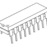
PIC16LF1847-E/ML Microchip Technology, PIC16LF1847-E/ML Datasheet - Page 51

PIC16LF1847-E/ML
Manufacturer Part Number
PIC16LF1847-E/ML
Description
14 KB Flash, 1K Bytes RAM, 32 MHz Int. Osc, 16 I/0, Enhanced Mid Range Core, Nan
Manufacturer
Microchip Technology
Series
PIC® XLP™ mTouch™ 16Fr
Datasheet
1.PIC16F1847-EP.pdf
(408 pages)
Specifications of PIC16LF1847-E/ML
Core Processor
PIC
Core Size
8-Bit
Speed
32MHz
Connectivity
I²C, LIN, SPI, UART/USART
Peripherals
Brown-out Detect/Reset, POR, PWM, WDT
Number Of I /o
15
Program Memory Size
14KB (8K x 14)
Program Memory Type
FLASH
Eeprom Size
256 x 8
Ram Size
1K x 8
Voltage - Supply (vcc/vdd)
1.8 V ~ 3.6 V
Data Converters
A/D 12x10b
Oscillator Type
Internal
Operating Temperature
-40°C ~ 125°C
Package / Case
28-VQFN Exposed Pad
Core
PIC
Processor Series
PIC16LF
Data Bus Width
8 bit
Maximum Clock Frequency
32 MHz
Data Ram Size
256 B
Number Of Programmable I/os
15
Number Of Timers
ÿ4 x 8-bit, 1 x 16-bit
Operating Supply Voltage
1.8 V to 5.5 V
Mounting Style
Through Hole
Interface Type
SPI, I2C
Lead Free Status / Rohs Status
Lead free / RoHS Compliant
- Current page: 51 of 408
- Download datasheet (4Mb)
4.2
Code protection allows the device to be protected from
unauthorized access. Program memory protection and
data EEPROM protection are controlled independently.
Internal access to the program memory and data
EEPROM are unaffected by any code protection
setting.
4.2.1
The entire program memory space is protected from
external reads and writes by the CP bit in Configuration
Word 1. When CP = 0, external reads and writes of
program memory are inhibited and a read will return all
‘0’s. The CPU can continue to read program memory,
regardless of the protection bit settings. Writing the
program memory is dependent upon the write
protection
Protection”
4.2.2
The entire data EEPROM is protected from external
reads and writes by the CPD bit. When CPD = 0, exter-
nal reads and writes of data EEPROM are inhibited.
The CPU can continue to read and write data EEPROM
regardless of the protection bit settings.
4.3
Write protection allows the device to be protected from
unintended self-writes. Applications, such as boot-
loader software, can be protected while allowing other
regions of the program memory to be modified.
The WRT<1:0> bits in Configuration Word 2 define the
size of the program memory block that is protected.
4.4
Four memory locations (8000h-8003h) are designated
as ID locations where the user can store checksum or
other code identification numbers. These locations are
readable and writable during normal execution. See
Section 11.5 “User ID, Device ID and Configuration
Word Access”
these memory locations. For more information on
checksum
“PIC16F/LF1847/PIC12F/LF1840
Programming Specification” (DS41439).
2011 Microchip Technology Inc.
Code Protection
Write Protection
User ID
PROGRAM MEMORY PROTECTION
DATA EEPROM PROTECTION
for more information.
setting.
for more information on accessing
calculation,
See
Section 4.3
see
Memory
“Write
Preliminary
the
PIC16(L)F1847
DS41453B-page 51
Related parts for PIC16LF1847-E/ML
Image
Part Number
Description
Manufacturer
Datasheet
Request
R

Part Number:
Description:
IC, 8BIT MCU, PIC16LF, 32MHZ, QFN-28
Manufacturer:
Microchip Technology
Datasheet:

Part Number:
Description:
IC, 8BIT MCU, PIC16LF, 32MHZ, QFN-28
Manufacturer:
Microchip Technology
Datasheet:

Part Number:
Description:
IC, 8BIT MCU, PIC16LF, 32MHZ, DIP-18
Manufacturer:
Microchip Technology
Datasheet:

Part Number:
Description:
IC, 8BIT MCU, PIC16LF, 20MHZ, TQFP-44
Manufacturer:
Microchip Technology
Datasheet:

Part Number:
Description:
7 KB Flash, 384 Bytes RAM, 32 MHz Int. Osc, 16 I/0, Enhanced Mid Range Core, Nan
Manufacturer:
Microchip Technology

Part Number:
Description:
14KB Flash, 512B RAM, LCD, 11x10b ADC, EUSART, NanoWatt XLP 28 SOIC .300in T/R
Manufacturer:
Microchip Technology
Datasheet:

Part Number:
Description:
14KB Flash, 512B RAM, LCD, 11x10b ADC, EUSART, NanoWatt XLP 28 SSOP .209in T/R
Manufacturer:
Microchip Technology
Datasheet:

Part Number:
Description:
MCU PIC 14KB FLASH XLP 28-SSOP
Manufacturer:
Microchip Technology

Part Number:
Description:
MCU PIC 14KB FLASH XLP 28-SOIC
Manufacturer:
Microchip Technology

Part Number:
Description:
MCU PIC 512B FLASH XLP 28-UQFN
Manufacturer:
Microchip Technology

Part Number:
Description:
MCU PIC 14KB FLASH XLP 28-SPDIP
Manufacturer:
Microchip Technology

Part Number:
Description:
MCU 7KB FLASH 256B RAM 40-UQFN
Manufacturer:
Microchip Technology

Part Number:
Description:
MCU 7KB FLASH 256B RAM 44-TQFP
Manufacturer:
Microchip Technology

Part Number:
Description:
MCU 14KB FLASH 1KB RAM 28-UQFN
Manufacturer:
Microchip Technology

Part Number:
Description:
MCU PIC 14KB FLASH XLP 40-UQFN
Manufacturer:
Microchip Technology


