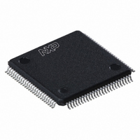
TDA9955HL/17/C1:55 NXP Semiconductors, TDA9955HL/17/C1:55 Datasheet - Page 10

TDA9955HL/17/C1:55
Manufacturer Part Number
TDA9955HL/17/C1:55
Description
TDA9955HL/LQFP100/TRAYBDP//17/
Manufacturer
NXP Semiconductors
Type
Videor
Datasheet
1.TDA9955HL17C151.pdf
(52 pages)
Specifications of TDA9955HL/17/C1:55
Resolution (bits)
8 b
Sampling Rate (per Second)
170M
Data Interface
Serial
Voltage Supply Source
Analog and Digital
Voltage - Supply
1.75 V ~ 1.85 V, 3.15 V ~ 3.45 V
Operating Temperature
0°C ~ 70°C
Mounting Type
Surface Mount
Package / Case
100-LQFP
Lead Free Status / RoHS Status
Lead free / RoHS Compliant
Other names
935281545551
TDA9955HL/17/C1-S
TDA9955HL/17/C1-S
TDA9955HL/17/C1-S
TDA9955HL/17/C1-S
Available stocks
Company
Part Number
Manufacturer
Quantity
Price
Company:
Part Number:
TDA9955HL/17/C1:55
Manufacturer:
NXP Semiconductors
Quantity:
10 000
NXP Semiconductors
9. I
TDA9955HL_1
Product data sheet
2
C-bus interface
8.13 Video port selection
8.14 Output buffers
8.15 VHREF timing generator
8.16 I
8.17 Power management
8.18 Sync timing measurement
9.1 I
Each channel (R or G or B in RGB 4 : 4 : 4 mode, Y or C
Y or C
affected to a specified video port VPA, VPB or VPC via the I
The levels of the output buffers are LV-TTL compatible. The switch of the outputs between
active and high-impedance is set by the I
The VHREF timing generator outputs all the timing signals used by the device: gain and
clamp pulses for calibration, coast signal to manage the PLL, VREF, HREF and FREF
signals for SAV/EAV and other, VS and HS signals to change width and position
compared with the synchronization inputs.
The I
slave address of the device is selected by pin A0. The programmed values in the registers
remain valid.
Only the serial interface (and the I
up in all cases even in the case when the device is set to power-down with the
PD-registers.
To assist the recognition of the input format, the vertical and horizontal periods are
measured based on the externally provided MCLK frequency (13.5 MHz). The width of the
horizontal pulse is also measured.
The TDA9955HL is a slave I
and protocol for I
Bit A0 of the I
I
Table 3.
Device address
A6
1
2
2
2
C-bus address is given in
C-bus serial interface
C-bus protocol
2
B
C-bus serial interface allows to program the internal registers of the device. The
C
R
in 4 : 2 : 2 semi-planar mode, C
I
2
A5
0
C-bus slave address
2
C-bus device address is externally selected by the A0 pin. The main device
2
C-bus are standard.
A4
0
Rev. 01 — 17 March 2008
Table
2
C-bus device and the SCL pin is only an input pin. The timing
Triple 8-bit analog-to-digital video converter for HDTV
3.
2
A3
1
C-bus registers) and the activity detection are powered
2
C-bus.
B
YC
A2
1
R
Y in 4 : 2 : 2 ITU-R BT.656 mode) can be
A1
1
B
or C
2
C-bus.
R
TDA9955HL
in YUV 4 : 4 : 4 mode,
A0
A0
© NXP B.V. 2008. All rights reserved.
R/W
-
0/1
10 of 52


