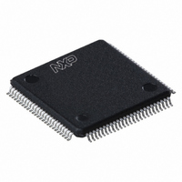
TDA9955HL/17/C1:55 NXP Semiconductors, TDA9955HL/17/C1:55 Datasheet - Page 31

TDA9955HL/17/C1:55
Manufacturer Part Number
TDA9955HL/17/C1:55
Description
TDA9955HL/LQFP100/TRAYBDP//17/
Manufacturer
NXP Semiconductors
Type
Videor
Datasheet
1.TDA9955HL17C151.pdf
(52 pages)
Specifications of TDA9955HL/17/C1:55
Resolution (bits)
8 b
Sampling Rate (per Second)
170M
Data Interface
Serial
Voltage Supply Source
Analog and Digital
Voltage - Supply
1.75 V ~ 1.85 V, 3.15 V ~ 3.45 V
Operating Temperature
0°C ~ 70°C
Mounting Type
Surface Mount
Package / Case
100-LQFP
Lead Free Status / RoHS Status
Lead free / RoHS Compliant
Other names
935281545551
TDA9955HL/17/C1-S
TDA9955HL/17/C1-S
TDA9955HL/17/C1-S
TDA9955HL/17/C1-S
Available stocks
Company
Part Number
Manufacturer
Quantity
Price
Company:
Part Number:
TDA9955HL/17/C1:55
Manufacturer:
NXP Semiconductors
Quantity:
10 000
NXP Semiconductors
Table 35.
Legend: * = default value
[1]
Table 36.
Legend: * = default value
TDA9955HL_1
Product data sheet
Addr Register
C8h
C9h
CAh
Addr Register
CBh
CCh
CDh
Fig 7.
Minimum width of the clamp pulse is 40 pixels and it must be active only during the horizontal back porch.
CLAMP_PIX_S_LSB 7 to 0 CLAMP_ PIX_ START[7:0]
CLAMP_PIX_MSB
CLAMP_PIX_E_LSB 7 to 0 CLAMP_PIX_ END[7:0]
CLP_F1_LINE_S_MSB 7 to 3 -
CLP_F1_LINE_S_LSB 7 to 0 CLAMP_F1_LINE_START[7:0]
CLP_F1_LINE_WIDTH 7 to 0 CLAMP_F1_LINE_WIDTH[7:0]
pixel 1
FREF in interlaced case
line 1
Clamp signal registers (address C8h to CAh) bit description
CLP_Fx_LINE_nnn registers (address CBh to D0h) bit description
FREF changes state at pixel 1
blanking period
Bit
7 to 4 CLAMP_ PIX_ START[11:8] W
3 to 0 CLAMP_ PIX_ END[11:8]
Bit
2 to 0 CLAMP_F1_ LINE_
Symbol
Symbol
START[10:8]
active video
active video
field 1
field 2
Rev. 01 — 17 March 2008
Triple 8-bit analog-to-digital video converter for HDTV
Access Value Description
W
W
W
Access Value Description
W
W
W
W
[1]
00h*
0h*
0h*
00h*
FREF
0
0000*
000*
00h*
00h*
clamp signal pixel start: position, in
number of pixels, of the beginning of
the clamp signal generated by the
timing generator
clamp signal pixel end: position, in
number of pixels, of the end of the
clamp signal generated by the timing
generator
FREF_F1_START[10:0]
LOW during field 1;
HIGH during field 2
(can be changed with bit FIELD_POL)
FREF_F2_START[10:0]
not used
clamp signal line start for
field 1 (LSB): position, in
number of lines, from which no
clamp pulses are generated for
field 1, typically during the
vertical pulse in case of the
sync on green signal
clamp signal line width for
field 1: width, in number of
lines, where no clamp pulses
are generated for field 1
TDA9955HL
© NXP B.V. 2008. All rights reserved.
001aaa293
31 of 52


