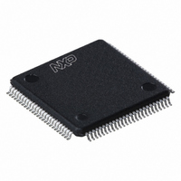
TDA9955HL/17/C1:55 NXP Semiconductors, TDA9955HL/17/C1:55 Datasheet - Page 9

TDA9955HL/17/C1:55
Manufacturer Part Number
TDA9955HL/17/C1:55
Description
TDA9955HL/LQFP100/TRAYBDP//17/
Manufacturer
NXP Semiconductors
Type
Videor
Datasheet
1.TDA9955HL17C151.pdf
(52 pages)
Specifications of TDA9955HL/17/C1:55
Resolution (bits)
8 b
Sampling Rate (per Second)
170M
Data Interface
Serial
Voltage Supply Source
Analog and Digital
Voltage - Supply
1.75 V ~ 1.85 V, 3.15 V ~ 3.45 V
Operating Temperature
0°C ~ 70°C
Mounting Type
Surface Mount
Package / Case
100-LQFP
Lead Free Status / RoHS Status
Lead free / RoHS Compliant
Other names
935281545551
TDA9955HL/17/C1-S
TDA9955HL/17/C1-S
TDA9955HL/17/C1-S
TDA9955HL/17/C1-S
Available stocks
Company
Part Number
Manufacturer
Quantity
Price
Company:
Part Number:
TDA9955HL/17/C1:55
Manufacturer:
NXP Semiconductors
Quantity:
10 000
NXP Semiconductors
TDA9955HL_1
Product data sheet
8.10 4 : 2 : 2 downsample filters
8.11 Range control
8.12 4 : 2 : 2 formatter
8.9 Color conversion
The origin of those pulses can be the VHREF timing generator or the SDRS block.
The color conversion allows an RGB signal coming from the analog video interface to
convert into YUV format or to convert a YUV signal coming from the analog video
interface into an RGB format. The color matrix formula is:
Activation of the matrix function and programming of all coefficients is made by I
These filters downsample the U and V signals with a factor 2.
A delay is added on the G/Y channel corresponding to the pipeline delay of the filters to
put the Y channel in phase with the UV channel.
Four filters are selectable by I
digital filter.
The range control function truncates the range of data at specified ceiling and floor values
to remove super-white and super-black pixels.
The 4 : 2 : 2 formatter contains the YUV 4 : 2 : 2 semi-planar and the YUV 4 : 2 : 2
ITU-R BT.656 formatting functions. The choice between these functions is done using the
I
YUV 4 : 2 : 2 semi-planar formatting function to put the Y channel in phase with the
UV channel.
In the case of the YUV 4 : 2 : 2, the data frequency corresponding to the Y signal is at
pixel clock frequency and the data frequency corresponding to the U and V signals is at
half the pixel clock frequency. For semi-planar, the output clock should be at the same
frequency as the pixel clock and for ITU-R BT.656 at the same frequency as the formatter
clock (double of the pixel-clock).
The Start Active Video (SAV) and End Active Video (EAV) timing reference codes can be
included in the data stream according the HREF, VREF and FREF signal positions from
the VHREF timing generator.
Specific codes programmed via the I
blanking period to mask gain and clamp calibration.
2
UB
YG
VR
C-bus. A delay is added on the G/Y channel corresponding to the pipeline delay of the
=
C
C
C
11
21
31
C
C
C
12
22
32
C
C
C
13
23
33
Rev. 01 — 17 March 2008
GY
BU
RV
2
C-bus, from the simple cut to the ITU-R BT.656 compliant
Triple 8-bit analog-to-digital video converter for HDTV
–
Oin
Oin
Oin
2
C-bus can replace the data stream during the
1
2
3
+
Oout
Oout
Oout
1
2
3
TDA9955HL
© NXP B.V. 2008. All rights reserved.
2
C-bus.
9 of 52


