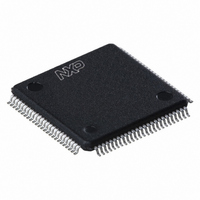
TDA9955HL/17/C1:55 NXP Semiconductors, TDA9955HL/17/C1:55 Datasheet - Page 43

TDA9955HL/17/C1:55
Manufacturer Part Number
TDA9955HL/17/C1:55
Description
TDA9955HL/LQFP100/TRAYBDP//17/
Manufacturer
NXP Semiconductors
Type
Videor
Datasheet
1.TDA9955HL17C151.pdf
(52 pages)
Specifications of TDA9955HL/17/C1:55
Resolution (bits)
8 b
Sampling Rate (per Second)
170M
Data Interface
Serial
Voltage Supply Source
Analog and Digital
Voltage - Supply
1.75 V ~ 1.85 V, 3.15 V ~ 3.45 V
Operating Temperature
0°C ~ 70°C
Mounting Type
Surface Mount
Package / Case
100-LQFP
Lead Free Status / RoHS Status
Lead free / RoHS Compliant
Other names
935281545551
TDA9955HL/17/C1-S
TDA9955HL/17/C1-S
TDA9955HL/17/C1-S
TDA9955HL/17/C1-S
Available stocks
Company
Part Number
Manufacturer
Quantity
Price
Company:
Part Number:
TDA9955HL/17/C1:55
Manufacturer:
NXP Semiconductors
Quantity:
10 000
NXP Semiconductors
Table 58.
V
values measured at V
otherwise specified.
TDA9955HL_1
Product data sheet
Symbol
Clamps
N
M
Phase-locked loop (PLL) of analog video part
t
N
f
f
ADCs (+ AGCs)
f
INL
DNL
S/N
Clock timing input (CKEXT)
f
Clock timing output (VCLK)
f
Horizontal timing output (HS)
t
Timing output (VPA0 to VPA7, VPB0 to VPB7, VPC0 to VPC7), see
t
t
t
TTL digital inputs (HCSYNC1, HCSYNC2, VSYNC1, VSYNC2 and CKEXT)
V
V
I
t
t
jit(PLL)(p-p)
clk(ref)
clk(o)(PLL)
s
clk(max)
clk(max)
d(pipe)
d(s)
su(Q)
h(Q)
i
r
f
DDA(3V3)
clk
clk
IL
IH
CL
pix
CL(CTC)
step
= V
Characteristics
DDI(3V3)
Parameter
clamping accuracy
channel-to-channel clamp matching
peak-to-peak PLL jitter time
number of pixels
reference clock frequency
PLL output clock frequency
phase difference
phase shift step
sampling frequency
integral non-linearity
differential non-linearity
signal-to-noise ratio
maximum clock frequency
clock duty cycle
maximum clock frequency
clock duty cycle
pipeline delay time
sampling delay time
data output set-up time
data output hold time
LOW-level input voltage
HIGH-level input voltage
input current
rise time
fall time
= V
DDA(3V3)
DDO(3V3)
…continued
= V
= 3.15 V to 3.45 V; V
DDI(3V3)
= V
DDO(3V3)
Rev. 01 — 17 March 2008
= 3.3 V, V
DDA(1V8)
Conditions
f
pixels per line
standard at 170 MHz
manual controls; T
maximum
f
f
without harmonics; f
sinewave input; f
analog inputs; RGB/YUV/YUV
4 : 2 : 2
semi-planar/ITU-R BT.656
horizontal sync pulse delay; in
phase with data outputs
referenced to VCLK
V
20 % to 80 %
80 % to 20 %
s
s
s
I
= 170 MHz; during 3 s
= 170 MHz
= 170 MHz
= 0 V or V
Triple 8-bit analog-to-digital video converter for HDTV
= V
DDA(1V8)
DDC(1V8)
I
= V
Figure 10
= V
s
= 1.75 V to 1.85 V; T
DD
DDC(1V8)
= 170 MHz
amb
i
= 1 MHz;
= 25 C
= 1.8 V and T
[1]
Min
-
-
-
256
15
12.5
-
-
170
-
-
-
170
-
170
45
-
-
-
2
-
2.0
-
-
-
amb
TDA9955HL
amb
= 0 C to 70 C; typical
= 25 C; unless
Typ
0.1
1.14
0.16
-
-
-
2.7
11.25 -
-
45
-
50
-
50
15.4
3.2
-
-
-
-
-
-
-
0.5
0.7
© NXP B.V. 2008. All rights reserved.
Max
1.8
1.20
1.60
4095 -
65
170
4.2
-
-
-
-
-
-
-
55
-
-
4.5
-
0.8
5.5
3
3
5
Unit
LSB
LSB
ns
kHz
MHz
step
deg
MHz
LSB
LSB
dB
MHz
%
MHz
%
clock
interval
ns
ns
ns
V
V
ns
ns
43 of 52
A


