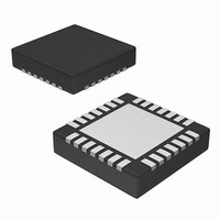
IDT5V49EE702NDGI8 IDT, Integrated Device Technology Inc, IDT5V49EE702NDGI8 Datasheet - Page 12

IDT5V49EE702NDGI8
Manufacturer Part Number
IDT5V49EE702NDGI8
Description
IC PLL CLK GEN 200MHZ 28VQFN
Manufacturer
IDT, Integrated Device Technology Inc
Type
Clock Generator, Multiplexerr
Datasheet
1.IDT5V49EE702NDGI8.pdf
(34 pages)
Specifications of IDT5V49EE702NDGI8
Pll
Yes with Bypass
Input
LVCMOS, LVTTL, Crystal
Output
HCSL, LVCMOS, LVDS, LVPECL, LVTTL
Number Of Circuits
1
Ratio - Input:output
2:7
Differential - Input:output
No/Yes
Frequency - Max
500MHz
Divider/multiplier
Yes/Yes
Voltage - Supply
3.135 V ~ 3.465 V
Operating Temperature
-40°C ~ 85°C
Mounting Type
Surface Mount
Package / Case
28-VQFN Exposed Pad, 28-HVQFN, 28-SQFN, 28-DHVQFN
Frequency-max
500MHz
Lead Free Status / RoHS Status
Lead free / RoHS Compliant
Other names
IDT5V49EE702DLGI8
IDT5V49EE702DLGI8
IDT5V49EE702DLGI8
SEL[2:0] Function
The IDT5V49EE702 can support up to six unique
configurations. Users may pre-programmed all these
configurations, and select the configurations using SEL[2:0]
SD/OE Pin Function
The polarity of the SD/OE signal pin can be programmed to
be either active HIGH or LOW with the SP bit (0x02). When
SP is “0” (default), the pin becomes active HIGH and when
SP is “1”, the pin becomes active LOW. The SD/OE pin can
be configured as either to shutdown the PLLs or to
enable/disable the outputs.
1 Assert to disable the outputs whose OE bits are set
2 Assert to shut down power, on the outputs and 3-level pins
Configuration OUTx IO Standard
Users can configure the individual output IO standard from
a specified 1.8V to 3.3V power supplies. Each output can
support 1.8V to 3.3V LVTTL. Each output pair can support
LVDS, LVPECL or HCSL from the specified 3.3V power
supply. OUT0 can only be 3.3V single-ended output.
Programming the Device
I
IDT® EEPROM PROGRAMMABLE CLOCK GENERATOR
2
C may be used to program the IDT5V49EE702.
IDT5V49EE702
EEPROM PROGRAMMABLE CLOCK GENERATOR
S D /O E
SEL2
0
0
0
0
1
1
1
1
S P
SEL1
S H
0
0
1
1
0
0
1
1
O E M o d e
SEL0
0
1
0
1
0
1
0
1
S D M o d e
1
Select CONFIG0
Select CONFIG1
Select CONFIG2
Select CONFIG3
Select CONFIG4
Select CONFIG5
Reserved (Do not use)
Reserved (Do not use)
2
12
pins. Alternatively, users may use I
these registers on-the-fly.
– Device (slave) address = 7'b1101010
I
The IDT5V49EE702 is programmed through an I
serial interface, and is an I
write transfer formats are supported. The first byte of data
after a write frame to the correct slave address is interpreted
as the register address; this address auto-increments after
each byte written or read.
The frame formats are shown in the following illustration.
2
Configuration Selections
C Programming
Framing
2
C slave device. The read and
IDT5V49EE702
2
CLOCK SYNTHESIZER
C interface to configure
REV F 022310
2
C-Bus


