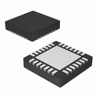
IDT5V49EE702NDGI8 IDT, Integrated Device Technology Inc, IDT5V49EE702NDGI8 Datasheet - Page 19

IDT5V49EE702NDGI8
Manufacturer Part Number
IDT5V49EE702NDGI8
Description
IC PLL CLK GEN 200MHZ 28VQFN
Manufacturer
IDT, Integrated Device Technology Inc
Type
Clock Generator, Multiplexerr
Datasheet
1.IDT5V49EE702NDGI8.pdf
(34 pages)
Specifications of IDT5V49EE702NDGI8
Pll
Yes with Bypass
Input
LVCMOS, LVTTL, Crystal
Output
HCSL, LVCMOS, LVDS, LVPECL, LVTTL
Number Of Circuits
1
Ratio - Input:output
2:7
Differential - Input:output
No/Yes
Frequency - Max
500MHz
Divider/multiplier
Yes/Yes
Voltage - Supply
3.135 V ~ 3.465 V
Operating Temperature
-40°C ~ 85°C
Mounting Type
Surface Mount
Package / Case
28-VQFN Exposed Pad, 28-HVQFN, 28-SQFN, 28-DHVQFN
Frequency-max
500MHz
Lead Free Status / RoHS Status
Lead free / RoHS Compliant
Other names
IDT5V49EE702DLGI8
IDT5V49EE702DLGI8
IDT5V49EE702DLGI8
DC Electrical Characteristics for LVDS
Power Supply Characteristics for LVDS Outputs
DC Electrical Characteristics for LVPECL
Power Supply Characteristics for LVPECL Outputs
IDT® EEPROM PROGRAMMABLE CLOCK GENERATOR
Symbol
Symbol
Symbol
Symbol
V
IDT5V49EE702
EEPROM PROGRAMMABLE CLOCK GENERATOR
V
V
I
I
I
SWING
I
I
OT
V
I
V
OT
V
I
OSD
DDQ
DDD
DDQ
DDD
TOT
OS
V
V
OS
OH
OL
OS
(+)
OT
(-)
Note 1: Output bank 5 is toggling. Other output banks are powered down.
Note 2: The termination resistors are excluded from these measurements.
Differential Output Voltage for the TRUE binary state
Differential Output Voltage for the FALSE binary state
Change in V
Output Common Mode Voltage (Offset Voltage)
Change in V
Outputs Short Circuit Current, V
Differential Outputs Short Circuit Current, V
Quiescent V
Supply Current
Dynamic V
Current per Output
Total Power V
Current
Output Voltage HIGH, terminated through 50Ω tied to V
Output Voltage LOW, terminated through 50Ω tied to V
Peak-to-Peak Output Voltage Swing
Quiescent V
Supply Current
Dynamic V
Current per Output
Parameter
Parameter
DD
DD
OT
OS
DD
DD
DD
Power Supply
Power Supply
between Complimentary Output States
Power
Power
between Complimentary Output States
Supply
Parameter
Parameter
REF = LOW
Outputs enabled, all outputs unloaded
V
F
F
F
REF = LOW
Outputs enabled, all outputs unloaded
V
REFERENCE CLOCK
REFERENCE CLOCK
REFERENCE CLOCK
OUT
DD
DD
= Max., C
= Max., C
+ or V
OUT
Test Conditions
Test Conditions
OUT
L
L
- = 0V or V
= 0pF
= 0pF
+ = V
19
= 100 MHz, C
= 200 MHz, C
= 400 MHz, C
OUT
DD
DD
-
DD
-2 V
-2 V
1
2
2
L
L
L
1
= 5 pF
= 5 pF
= 5 pF
V
V
DD
1.125
DD
Min
-247
Min
0.55
247
-1.95
-1.2
Typ
Typ
100
122
68
30
86
86
35
Typ
Typ
1.2
9
6
IDT5V49EE702
CLOCK SYNTHESIZER
Max
Max
130
150
190
110
90
45
50
V
V
DD
1.375
Max
Max
DD
-454
0.93
454
50
50
24
12
-1.61
-0.9
REV F 022310
µA/MHz
µA/MHz
Unit
Unit
mA
mA
mA
Unit
Unit
mV
mV
mV
mV
mA
mA
V
V
V
V


