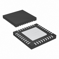
MAX1020BETX+ Maxim Integrated Products, MAX1020BETX+ Datasheet - Page 2

MAX1020BETX+
Manufacturer Part Number
MAX1020BETX+
Description
IC ADC/DAC 10BIT 36-TQFN-EP
Manufacturer
Maxim Integrated Products
Type
ADC, DACr
Datasheet
1.MAX1020BETX.pdf
(44 pages)
Specifications of MAX1020BETX+
Resolution (bits)
10 b
Sampling Rate (per Second)
225k
Data Interface
MICROWIRE™, QSPI™, Serial, SPI™
Voltage Supply Source
Analog and Digital
Voltage - Supply
4.75 V ~ 5.25 V
Operating Temperature
-40°C ~ 85°C
Mounting Type
Surface Mount
Package / Case
36-TQFN Exposed Pad
Lead Free Status / RoHS Status
Lead free / RoHS Compliant
10-Bit, Multichannel ADCs/DACs with FIFO,
Temperature Sensing, and GPIO Ports
ABSOLUTE MAXIMUM RATINGS
AV
DGND to AGND.....................................................-0.3V to +0.3V
DV
Digital Inputs to DGND.............................................-0.3V to +6V
Digital Outputs to DGND .........................-0.3V to (DV
Analog Inputs, Analog Outputs and REF_
Maximum Current into Any Pin (except AGND, DGND, AV
Maximum Current into OUT_.............................................100mA
ELECTRICAL CHARACTERISTICS
(AV
(MAX1020/MAX1022/MAX1058), external reference V
T
(MAX1020/MAX1022/MAX1058), T
Note: If the package power dissipation is not exceeded, one output at a time may be shorted to AV
Stresses beyond those listed under “Absolute Maximum Ratings” may cause permanent damage to the device. These are stress ratings only, and functional
operation of the device at these or any other conditions beyond those indicated in the operational sections of the specifications is not implied. Exposure to
absolute maximum rating conditions for extended periods may affect device reliability.
2
DC ACCURACY (Note 1)
Resolution
Integral Nonlinearity
Differential Nonlinearity
Offset Error
Gain Error
Gain Temperature Coefficient
Channel-to-Channel Offset
D YN A M IC SPEC IF I C A T IO N S ( 1 0 k H z s in e - w a v e in p u t , V
2 2 5 k s p s , f
Signal-to-Noise Plus Distortion
Total Harmonic Distortion
(Up to the Fifth Harmonic)
Spurious-Free Dynamic Range
Intermodulation Distortion
Full-Linear Bandwidth
Full-Power Bandwidth
CONVERSION RATE (Note 3)
Power-Up Time
A
to AGND...............................................-0.3V to (AV
DV
DD
DD
= -40°C to +85°C, unless otherwise noted. Typical values are at AV
DD
_______________________________________________________________________________________
DD
to AGND .........................................................-0.3V to +6V
to AV
indefinitely
= DV
, and OUT_) ...........................................................50mA
PARAMETER
SC LK
DD
DD
.......................................................-3.0V to +0.3V
= 3 .6 M H z)
= 2.7V to 3.6V (MAX1057), external reference V
A
= +25°C. Outputs are unloaded, unless otherwise noted.)
SYMBOL
SINAD
SFDR
DNL
THD
IMD
INL
t
PU
(Note 2)
f
SINAD > 70dB
-3dB point
External reference
Internal reference (Note 4)
IN1
= 9.9kHz, f
DD
DD
REF
+ 0.3V)
+ 0.3V)
IN
= 4.096V (MAX1020/MAX1022/MAX1058), f
DD
= 2 .5 V
,
CONDITIONS
IN2
ADC
P- P
= 10.2kHz
( M A X1 0 5 7 ) , V
Continuous Power Dissipation (T
Operating Temperature Range ...........................-40°C to +85°C
Storage Temperature Range .............................-60°C to +150°C
Junction Temperature ......................................................+150°C
Lead Temperature (soldering, 10s) .................................+300°C
REF
36-Pin Thin QFN (6mm x 6mm)
48-Pin Thin QFN (7mm x 7mm)
(derate 26.3mW/°C above +70°C) ......................2105.3mW
(derate 26.3mW/°C above +70°C) ......................2105.3mW
= 2.5V (MAX1057), AV
DD
IN
= DV
= 4 .0 9 6 V
DD
= 3V (MAX1057), AV
P- P
MIN
10
( M A X1 0 2 0 /M A X1 0 2 2 /M A X1 0 5 8 ) ,
CLK
DD
A
±0.025
±0.25
±0.5
±0.5
±1.4
±0.1
TYP
100
218
= +70°C)
-70
0.8
DD
61
66
72
= 3.6MHz (50% duty cycle),
1
= DV
, DV
DD
DD
MAX
±1.0
±1.0
±2.0
±2.0
, AGND, or DGND
= 4.75V to 5.25V
DD
= DV
C onver si on
ppm/°C
UNITS
C ycl es
DD
C l ock
MHz
LSB
LSB
LSB
LSB
LSB
dBc
dBc
dBc
kHz
Bits
dB
µs
= 5V


