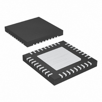
MAX1020BETX+ Maxim Integrated Products, MAX1020BETX+ Datasheet - Page 35

MAX1020BETX+
Manufacturer Part Number
MAX1020BETX+
Description
IC ADC/DAC 10BIT 36-TQFN-EP
Manufacturer
Maxim Integrated Products
Type
ADC, DACr
Datasheet
1.MAX1020BETX.pdf
(44 pages)
Specifications of MAX1020BETX+
Resolution (bits)
10 b
Sampling Rate (per Second)
225k
Data Interface
MICROWIRE™, QSPI™, Serial, SPI™
Voltage Supply Source
Analog and Digital
Voltage - Supply
4.75 V ~ 5.25 V
Operating Temperature
-40°C ~ 85°C
Mounting Type
Surface Mount
Package / Case
36-TQFN Exposed Pad
Lead Free Status / RoHS Status
Lead free / RoHS Compliant
Do not issue a second CNVST signal before EOC goes
low; otherwise, the FIFO can be corrupted. Wait until all
conversions are complete before reading the FIFO. SPI
communications to the DAC and GPIO registers are per-
mitted during conversion. However, coupled noise may
result in degraded ADC signal-to-noise ratio (SNR).
In clock mode 01, conversions are requested one at a
time using CNVST and performed automatically using
the internal oscillator. See Figure 7 for clock mode 01
timing after a command byte is issued.
Setting CNVST low begins an acquisition, wakes up the
ADC, and places it in track mode. Hold CNVST low for
Figure 6. Clock Mode 00—After writing a command byte, set CNVST low for at least 40ns to begin a conversion.
Figure 7. Clock Mode 01—After writing a command byte, request multiple conversions by setting CNVST low for each conversion.
Internally Timed Conversions with CNVST
CNVST
X = DON'T CARE.
DOUT
SCLK
CNVST
EOC
X = DON'T CARE.
DOUT
SCLK
CS
EOC
CS
(ACQUISITION 1)
(CONVERSION 1)
Externally Timed Acquisitions and
10-Bit, Multichannel ADCs/DACs with FIFO,
ADC Conversions in Clock Mode 01
______________________________________________________________________________________
t
DOV
(ACQUISITION 2)
Temperature Sensing, and GPIO Ports
t
CSW
(UP TO 514 INTERNALLY CLOCKED ACQUISITIONS AND CONVERSIONS)
t
RDS
(CONVERSION 2)
MSB1
MSB1
at least 1.4µs to complete the acquisition. If reference
mode 00 or 10 is selected, an additional 45µs is
required for the internal reference to power up. If a tem-
perature measurement is being requested, reference
power-up and temperature measurement is internally
timed. In this case, hold CNVST low for at least 40µs.
Set CNVST high to begin a conversion. Sampling is
completed approximately 500ns after CNVST goes
high. After the conversion is complete, the ADC shuts
down and pulls EOC low. EOC stays low until CS or
CNVST is pulled low again. Wait until EOC goes low
before pulling CS or CNVST low. The number of CNVST
signals must equal the number of conversions request-
ed by the scan and averaging registers to correctly
update the FIFO. Wait until all conversions are com-
plete before reading the FIFO. SPI communications to
the DAC and GPIO registers are permitted during con-
LSB1
LSB1
MSB2
MSB2
35


